Chinese semiconductor industry

Status
Not open for further replies.

ansy1968

Brigadier
Registered Member
Another one from @Oldschool ,he and I speculate that it may used Local Equipment. ;)

Oldschool

Junior Member​

Registered Member
Today at 3:07 PMNew
I am curious what type of equipments they use for manufacturing.

It's not a standard CMOS process and the news said it used self developed equipments.


Please, Log in or Register to view URLs content!

原文来源:杭州日报记者:管光前 叶佳裕 通讯员:刘方泽 周艳清虎年新春伊始,杭州青山湖科技城传来佳音。由昕原半导体(杭州)有限公司(以下称“昕原半导体”)主导建设的大陆首条28/22nm ReRAM(阻变存储器)12...
Please, Log in or Register to view URLs content!


  • It is expected to help the domestic new storage field to achieve "curve overtaking" The first resistive memory pilot test line in mainland China opens in Lin'an!
  • Release time: 2022-02-17 17:46 267
  • Original source: Hangzhou Daily
    Reporter: Guan Guangqian Ye Jiayu Correspondent: Liu Fangze and Zhou Yanqing

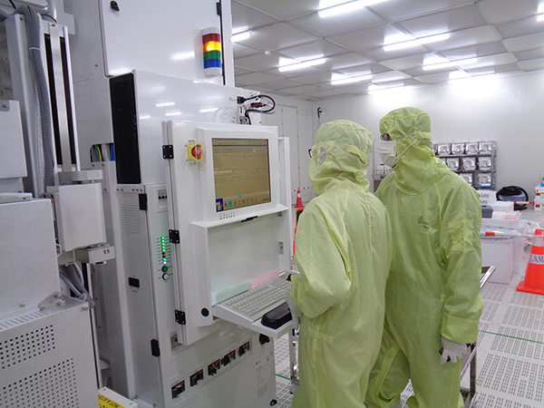
    At the beginning of the Chinese New Year of the Tiger Year, good news came from Hangzhou Qingshan Lake Science and Technology City. The first 28/22nm ReRAM (resistive variable memory) 12-inch pilot production line in mainland China , led by Xinyuan Semiconductor (Hangzhou) Co., Ltd. (hereinafter referred to as "Xinyuan Semiconductor") , has successfully completed the installation and acceptance of self-developed equipment. The process flow of the pilot line has been connected, and the film has been successfully taped out.
    WeChat picture_20220222172747-edited.png

    Xinyuan Semiconductor technicians conduct equipment debugging on the pilot line

    The new memory "Qianjing" is broad

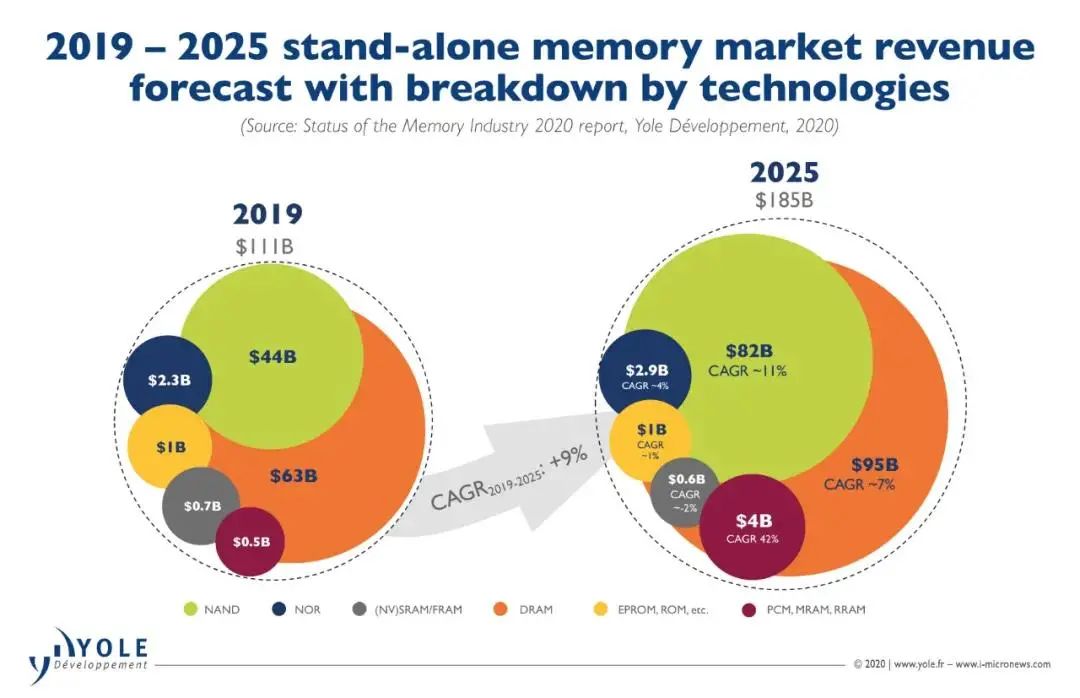
    In the national "14th Five-Year Plan" outline, in terms of strengthening original and leading scientific and technological research, "advanced storage technology upgrade" has been included in the key area of "research in frontier areas of science and technology". And according to the statistics of Yole Development, the world's authoritative semiconductor market research organization, the overall memory market space will increase from US$111 billion in 2019 to US$ 185 billion in 2025 .
    1645522443519055.jpg

    Global memory market size and growth rate (Source: YOLE)

    At present, my country is vigorously developing the storage industry: on the one hand, it is striving to catch up with traditional memory, such as YMTC, which fully invests in NAND Flash (a type of Flash memory) and focuses on DRAM (the most common system memory for dynamic random access memory). On the other hand, it is also laying out new types of memory in advance.

    With the advent of the era of the Internet of Everything, in response to the needs of future artificial intelligence (AI), smart cars, artificial intelligence and the Internet of Things (AIOT) and edge computing (Edge Computing) and other high computing capabilities, such as DRAM, NAND and other high-capacity memories. Flash memory's high power consumption and speed issues can no longer keep pace with the times. To put it simply, whether DRAM can be stored (data is lost after power failure), and whether NAND Flash can be stored (low read and write speed), if NAND+DRAM is used together, it will cause high energy consumption, and another common memory is Nor Due to the low storage density (low storage capacity) of Flash and the inability to embed processes below 28nm/22nm, it is difficult to achieve performance breakthroughs on the existing basis.

    Under the urgent needs of the market, it is imperative to develop and produce a new generation of memory that integrates high storage density, high speed, low power consumption, and can be embedded in processes below 28nm.

    Simple material, low cost, but unusual performance


    At present, the world's mainstream new memory technologies mainly include PCM (phase change memory), FeRAM (ferroelectric memory), MRAM (magnetic memory) and ReRAM (resistive change memory) . Compared to several other new memory technologies, ReRAM requires fewer types of materials and the number of additional masks, allowing for lower production costs. At the same time, the industry generally believes that ReRAM can fully meet the energy consumption, performance and storage density requirements of applications such as neuromorphic computing and edge computing, and is expected to be widely used in AIoT, smart cars, data centers, AI computing (integration of storage and computing) and other fields. use.

    1645522572651470.png

    The data-driven future has arrived

    "We are very optimistic about the technical and commercial development prospects of ReRAM memory from the aspects of density, energy efficiency ratio, cost, process and yield , so we make it our R&D focus!" said the relevant person in charge of Xinyuan Semiconductor.

    Domestic memory is expected to "overtake in corners"


    The core of the new type of memory is that in its development, it is necessary to add some special features to the traditional CMOS (abbreviation for complementary metal oxide semiconductor, a technology used to make large-scale integrated circuit chips or chips made with this technology) process. Materials or processes, the development of these special materials or processes needs to be verified by a lot of experiments and tests.

    Traditional CMOS foundries may be limited by resources, and the iteration speed is slow, which affects the progress of process development. Although major domestic research institutes can speed up the iteration speed in the laboratory stage, there is no standard 12-inch mass production line. , the experimental results are often difficult to mass production.

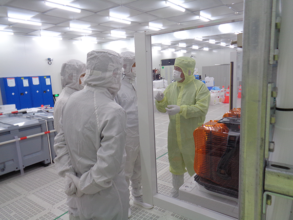
    Xinyuan's self-built 28/22nm ReRAM (resistive variable memory) 12-inch pilot production line solved the above problems. Drawing on the strengths of foundries and laboratories, it has fast iteration speed, flexible production lines, and independent and controllable intellectual property rights , making it possible to quickly realize ReRAM-related products.
    WeChat picture_20220216105655-edited.png

    Xinyuan Semiconductor technicians conduct equipment testing on the pilot line

    "As the first 28/22nm ReRAM 12-inch pilot production line in mainland China , the smooth turn-on of our production line and the completion of product verification and mass production will greatly promote the development of China's new storage industry." The relevant person in charge of Xinyuan Semiconductor said, "In this field, the gap between domestic and foreign countries is currently small, and barriers have not yet been formed, which provides the possibility for China's memory industry to achieve "curve overtaking" ."
Next:
Please, Log in or Register to view URLs content!
 

horse

Colonel
Registered Member
From @Oldschool, of the 3 core tech needed for an EUVL the Chinese solved two of them (optics and Dual stage bench) and are commercially applicable, meaning they're not research tool anymore BUT can be mass produced. the original power source the DPP is not powerful enough to be commercially viable and we have to wait for HEPS project to finished in 2025, a major breakthrough in LPP this year or a successful JV with Russia in 2024. ;)

[/HEADING]
[HEADING=3]Oldschool

Junior Member​

Registered Member
Today at 2:10 AMNew
xw.qq.com

Please, Log in or Register to view URLs content!

中国芯再加速!国产光刻机核心部件迎来突破,距离胜利又近了一步,如果要评选中国最急需突破的科技产品,恐怕非光刻机莫属,作为芯片制造流程中技术难度最大、成本最高、最难仿制的关键设备,光刻机已经成为“压制”中国科技进步的最大阻碍。全球唯一的EUV光刻机供应商、荷兰科……
xw.qq.com
xw.qq.com
Not sure if this is news to you but anyway
For EUV mirror for projection optics, changchun optic institute has solved the manufacturing issue.
就在近期,中国新闻网就报道了一则重大利好消息,长春光机所已经成功突破了光刻机核心部件“光学投影物镜”制造关键技术,实现了中国超精密光学技术的跨越式发展。

Synchrotron their ass!

That is enough power to zap all peasant asses, send us running!

:D
 

tokenanalyst

Brigadier
Registered Member

At least 5nm, China Great Wall announced the launch of fully automatic 12-inch wafer laser grooving equipment​


China Great Wall official micro announced that the company's Zhengzhou Rail Transit Information Technology Research Institute, based on the experience and basis of the development of semiconductor laser invisible wafer cutting equipment, has launched a new technology that supports full cutting of ultra-thin wafers. Fully automatic 12-inch wafer laser grooving equipment for the process .
China Great Wall Announces Fully Automatic 12-inch Wafer Laser Slotting Equipment

▲ Source: Great Wall of China
According to reports, in addition to the conventional laser grooving function, the device also supports 5nm DBG process , ultra-thin wafer full cutting function below 120 microns, fab IGBT process side related processes and TAIKO ultra-thin ring cutting and other high-precision end process.
IT House learned that the Great Wall of China official stated that the modular design of the device can support lasers with different pulse widths (nanosecond, picosecond, femtosecond). The self-developed optical system can realize continuous adjustment of the width and length of the spot. With the high-precision motion control platform and other technologies, it is combined with the laser stealth cutting equipment to solve the problems of laser stealth cutting equipment on surface material, thickness, crystal orientation and resistivity. Limit, help control product breakage rate and improve chip yield.
 

ansy1968

Brigadier
Registered Member

At least 5nm, China Great Wall announced the launch of fully automatic 12-inch wafer laser grooving equipment​


China Great Wall official micro announced that the company's Zhengzhou Rail Transit Information Technology Research Institute, based on the experience and basis of the development of semiconductor laser invisible wafer cutting equipment, has launched a new technology that supports full cutting of ultra-thin wafers. Fully automatic 12-inch wafer laser grooving equipment for the process .
China Great Wall Announces Fully Automatic 12-inch Wafer Laser Slotting Equipment

▲ Source: Great Wall of China
According to reports, in addition to the conventional laser grooving function, the device also supports 5nm DBG process , ultra-thin wafer full cutting function below 120 microns, fab IGBT process side related processes and TAIKO ultra-thin ring cutting and other high-precision end process.
IT House learned that the Great Wall of China official stated that the modular design of the device can support lasers with different pulse widths (nanosecond, picosecond, femtosecond). The self-developed optical system can realize continuous adjustment of the width and length of the spot. With the high-precision motion control platform and other technologies, it is combined with the laser stealth cutting equipment to solve the problems of laser stealth cutting equipment on surface material, thickness, crystal orientation and resistivity. Limit, help control product breakage rate and improve chip yield.
@tokenanalyst bro they're delving their hands or to research the 5nm tech in advance while preparing the 7nm localization line next year. Boy Oi Boy IF this pattern continue then I speculate that we may see the mythical SSA900 22nm DUVL makes its appearance in 2023 with localized 5nm line in 2024.
 

tokenanalyst

Brigadier
Registered Member
@tokenanalyst bro they're delving their hands or to research the 5nm tech in advance while preparing the 7nm localization line next year. Boy Oi Boy IF this pattern continue then I speculate that we may see the mythical SSA900 22nm DUVL makes its appearance in 2023 with localized 5nm line in 2024.
I think 5nm is maybe a bit of a stretch but who knows, but yeah the patent activity of SMEE, CHEERTECH, RSLASER, U-Precision, Guowang Optical and so on has going up significantly between this and last year, they may gearing up to mass produce components for immersion and multiple types of lithography systems.
 

tokenanalyst

Brigadier
Registered Member
Anji Microelectronics Technology (Shanghai) Co., Ltd. is a high-tech semiconductor material company based on independent innovation, integrating R&D, production, sales and technical services. The company's main business is the research and development and industrialization of key semiconductor materials. Its current products include different series of chemical mechanical polishing liquids and photoresist removers, which are mainly used in the field of integrated circuit chip manufacturing and advanced packaging.

chemical mechanical polishing fluid

Chemical mechanical polishing is a key process to achieve uniform global planarization of wafers in the manufacturing process of integrated circuit chips, and chemical mechanical polishing liquid is the main chemical material used in the chemical mechanical polishing process. The company's chemical mechanical polishing solution has achieved large-scale sales in the 130-14nm technology node, mainly used in domestic 8-inch and 12-inch mainstream wafer production lines; 10-7nm technology node products are being developed. According to different polishing objects, the company's chemical mechanical polishing liquid includes copper and copper barrier series, tungsten polishing liquid, silicon polishing liquid, oxide polishing liquid and other products.

Please, Log in or Register to view URLs content!
 

KenC

Junior Member
Registered Member
Some news on Hua Hong production plant in Shanghai having to cope with the lockdown.


In order to ensure the production of semiconductor chips during the COVID-19 pandemic in Shanghai, more than 6,000 employees of Hua Hong Group, one of China's top 500 manufacturing companies, temporarily moved into the company’s Shanghai plant before the closed loop management came in force. They eat and live in the compound and overcome difficulties to ensure the production of chips.

During this wave of epidemic, 6,000 employees are sticking to their posts in five production lines of the factory. The engineers' office area is busy and bustling as normal, and the production lines are running at full capacity.

The special 8-inch chip production line is located in a dust-free workshop. Inside, one shift is composed nearly 200 employees, including production engineers, front-line personnel, and even representatives of the suppliers. Also, in the fully automatic 12-inch chip production line, there are more than 100 employees operating and maintaining the equipment. These people are working hard to ensure production amid rising COVID cases and strict control measures, which reduced available workforce of the plant by about 40%.

Chips are a crucial cornerstone of the national economy and it is an important material used in all walks of life. That’s why on the evening of March 27, as soon as the news of the closure and control in Pudong New Area was announced, more than 6,000 employees rushed back to the factory, some of whom traveling nearly 90 kilometers from Jinshan District before midnight. The plant compound is usually used for production and business only, but is now also serving as accommodation for all these people. There was no showering area in the compound, so the employees used their hands-on skills to find waterproof material and tools, and built a temporary shower house. The passages outside the workshops, offices, conference rooms and multi-functional rooms are now also ad-hoc domitories. It is under such difficult conditions that everyone is ensuring the output of chips while contributing to dealing with COVID-19.
 

tokenanalyst

Brigadier
Registered Member

Chip industry's expansion plans at risk as equipment delays grow​

TSMC, Samsung and others chase vital equipment as delivery times reach 18 months
https%253A%252F%252Fs3-ap-northeast-1.amazonaws.com%252Fpsh-ex-ftnikkei-3937bb4%252Fimages%252F5%252F0%252F6%252F5%252F39785605-1-eng-GB%252Fjpp04717623.jpg


Chipmakers trying to expand production capacity are having to wait a year and a half or longer for key equipment, as unprecedented parts shortages and supply constraints batter the chip tools industry.

Looks like an oppurtunity to local players to build capacity to meet the demand.
 
Status
Not open for further replies.
Top