Chinese semiconductor industry

Status
Not open for further replies.

supercat

Major
Study for building multifunctional molecular nanocircuits:

Single-molecule field effect and conductance switching driven by electric field and proton transfer​

Abstract

Single-molecule junctions (SMJs) offer a novel strategy for miniaturization of electronic devices. In this work, we realize a graphene-porphyrin-graphene SMJ driven by electric field and proton transfer in two configurations. In the transistor configuration with ionic liquid gating, an unprecedented field-effect performance is achieved with a maximum on/off ratio of ~4800 and a gate efficiency as high as ~179 mV/decade in consistence with the theoretical prediction. In the other configuration, controllable proton transfer, tautomerization switching, is directly observed with bias dependence. Room temperature proton transfer leads to a two-state conductance switching, and more precise tautomerization is detected, showing a four-state conductance switching at high bias voltages and low temperatures. Such an SMJ in two configurations provides new insights into not only building multifunctional molecular nanocircuits toward real applications but also deciphering the intrinsic properties of matters at the molecular scale.
Please, Log in or Register to view URLs content!
 

gelgoog

Lieutenant General
Registered Member
So the "domestic" Kunpeng chip is still dependent on US technology.
Those where manufactured by TSMC, do they shifted the fabrication to SMIC 14nm? or another 28nm fab?
There is no way this can happen or SMIC would get sanctioned themselves. Already proven when US threatened SMIC after they made 14nm chips for Huawei's smartphones. They had to stop production for Huawei.

The solution is production facility free of US technology. Allegedly the first one will be the fab SMIC is building in Beijing.
 

tokenanalyst

Brigadier
Registered Member
Huawei invests in another semiconductor equipment company!

According to the news on February 14,
Please, Log in or Register to view URLs content!
Hubble invested in Beijing Tesdi
Please, Log in or Register to view URLs content!
Equipment Co., Ltd. (hereinafter referred to as "Tesdi"), with a shareholding ratio of 10%, making it the fifth largest shareholder of Tesdi.
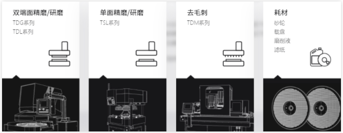
According to the information on the official website, Tesidi was established on March 19, 2020, and its legal representative is Liu Yongfeng. machine, metal plane polishing machine and brush-type plane deburring machine, providing customers with a complete set of technical processes and solutions such as fine grinding, grinding, polishing and deburring.
The company is guided by a flatter, thinner and faster technology, focusing on semiconductor substrate materials, semiconductor devices, advanced packaging, MEMS and other fields, providing system solutions and process equipment for thinning, polishing and CMP.
image.png

Picture (from the official website of Tesdy)

Invested many times in the field of equipment, involving
Please, Log in or Register to view URLs content!

It is worth noting that this is not the first time that Huawei Hubble has invested in the field of semiconductor equipment. Before that, it has invested in a number of semiconductor equipment companies. According to incomplete statistics, only last year (2021), Huawei Hubble invested in the field of semiconductor equipment. As many as 4 cases, the coverage is very wide. Specifically, it includes:
In June 2021, Keyi Hongyuan, a domestic high-end excimer laser technology manufacturer, added Huawei Hubble, Xuzhou Guangyuan Equity Investment Partnership (Limited Partnership) and natural person Jiang Rui, a subsidiary of Huawei, as the company's shareholders. At the same time, the registered capital increased from 120 million Yuan increased to 201.6 million yuan, an increase of 68%. Among them, Hubble Investment holds 4.7619%.

Please, Log in or Register to view URLs content!
 

tokenanalyst

Brigadier
Registered Member

Molten droplet generating device for EUV light source​

CN213876314U 2021

Shandong Aite Mechanical & Electrical Technology Co ltd.
Shanghai Institute of Optics and Fine Mechanics of CAS.


Abstract​

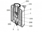
The utility model provides a molten liquid drop generating device for EUV light source, wherein the outer wall of the body is provided with a heat-conducting oil input port and a heat-conducting oil output port; the heating cavity is filled with heat conduction oil, and the electric heating rod extends into the heat conduction oil; an inner cavity is arranged in the inner cavity, the top of the inner cavity of the top cover is connected, a fixing cap is arranged in the inner cavity, a compression spring is fixed at the bottom of the fixing cap, a filter cap is arranged at the bottom of the compression spring, the bottom of the filter cap is communicated with an output channel, the output channel is connected with a high-speed sprayer, the high-speed sprayer is connected with a compression nut, and the compression nut is fixed at the bottom of the body; has the advantages that: the filtering cap of the utility model is used for removing metal impurities; the sealing ring and the compression spring maintain the melting device to be used in a high-temperature and high-pressure environment, and the inner cavity realizes the heating, melting and transmission of metal; the heating cavity is used for transmitting a heat-conducting medium; the electric heating rod maintains the whole experimental temperature environment of the melting device; the high-speed spray head sprays out metal liquid drops for experiments as required. the heating cavity is used for transmitting a heat-conducting medium; the electric heating rod maintains the whole experimental temperature environment of the melting device; the high-speed spray head sprays out metal liquid drops for experiments as required.t he heating cavity is used for transmitting a heat-conducting medium; the electric heating rod maintains the whole experimental temperature environment of the melting device; the high-speed spray head sprays out metal liquid drops for experiments as required.

1648307559486.png

This is the Second commercial company I have seen involved in EUV in China.
 

gelgoog

Lieutenant General
Registered Member
Photoresist chemicals, I think they managed to produce 7nm Photoresist. You need to understand that semiconductor is not just about lithography, it's about chemicals and other processes too.
From what I understand you need a different photoresist material according to the frequency of the light source.
So if it is ArF photoresist material it will work from 28nm all over to 7nm.
 

FairAndUnbiased

Brigadier
Registered Member
From what I understand you need a different photoresist material according to the frequency of the light source.
So if it is ArF photoresist material it will work from 28nm all over to 7nm.
well, it also has to do with whether it's for immersion or not. immersion resists either need a photochemically inert barrier topcoat and be chemically compatible with such, or they need to be completely insoluble in water both pre exposure and post exposure
Please, Log in or Register to view URLs content!
.
 

tokenanalyst

Brigadier
Registered Member
This is quite a big statement, considering that even litho machine to validate the photoresist at 7nm is very difficult to get.

Care to better explain why you think this?
i think 7nm come from Nata own statements.
Please, Log in or Register to view URLs content!

-Not very difficult, ASML is not restricted to sell even their most advanced DUVi machines to China, for now only EUV is restricted.
-7nm refers to the multi patterning process, most immersion machines are restricted to a feature size of ~38nm
, they probably tested trying to see if the photo-resists holds with features close together.
 
Status
Not open for further replies.
Top