They also do less advanced multi-axis motion stages (50-100nm in precision) for high precision manufacturing in other areas.this is the real deal here.
My guess packaging, micro-manufacturing, power and others.


They also do less advanced multi-axis motion stages (50-100nm in precision) for high precision manufacturing in other areas.this is the real deal here.
yes, 1 beamline = 1 EUV machine. Here's a diagram of what a synchrotron beamlines looks like.
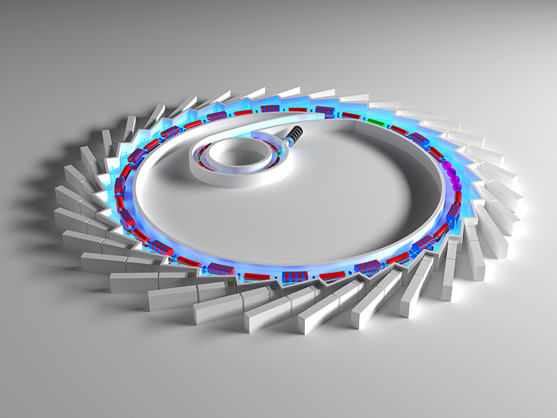
It would change fab layout and increase fab construction costs. It would also increase the difficulty of multiple EUV steps, since 1 mask = 1 step = 1 layer. However, in exchange you can have economies of scale with multiple EUV optics sets being serviced with 1 synchrotron. How many EUV instruments do you need?
At some point the cost of adding another EUV source (~$50 million per source) will outweigh the cost of having 1 big synchrotron ($172 million per 8 beamlines for the Shanghai synchrotron or $25 million per source if you use all 8).
")
So basically synchrotrons are extremely attractive to fab companies like TSMC but not to the equipment manufacturers like ASML? That explains why SSMB EUVL was not really explored - one side does not have the skillset to produce such systems, while the other simply does not want them because they are not as profitable. I hope this works out well for China, I am sure they can find enough land if the project overall is successful - make Xinjiang the semiconductor capital of the world and watch MuriKKKa seethe, j/k.
ASML tools cost more than Nikon ones. I had another source that was more recent but had broken English and no original, so I don't know the reliability, but it claimed that ASML costs were ~70 million and Nikon was 1/3 because they were desperate for sales.
I believe that China and Japan have much more similar cost structures in terms of average wages, taxes, infrastructure, social welfare, supply chain costs, etc. than Netherlands, so I believe SMEE tools will be priced similar to Canon and Nikon, rather than ASML.

I don't think so. The biggest buyer of Nikon DUV is Intel, they only sell a few dozen instruments per year (to Intel) and Canon DUV is outright worse than SMEE DUV. It use to be that DUV had multiple competitors in the early 2000's but Canon never got into ArF lithography and Nikon never got into EUV.Do Chinese companies buy DUV machines from Nikon or Canon ? is there any restrictions?
What the hell. Is this forum an advertisement for U-precision . This is the 4th time someone has posted this article. Please don't send it again .U-Precision
Beijing Huazhuo Jingke Technology Co., Ltd. was founded by the Tsinghua IC equipment team with the support of Tsinghua University and its subordinate "Beijing-Tsinghua Industrial Technology Research Institute" and the 02 special project. technology companies. The original intention of the establishment of the company is to industrialize the high-end monopoly technology accumulated by Tsinghua University in the 02 special project, and to provide the domestic market with high-end components and subsystem products that are urgently needed by the industry through the method of "technology radiation & downward". Huazhuo Jingke is mainly engaged in the research and development, design, production, sales and technical services of semiconductor manufacturing equipment and its key components.
The company has a registered capital of 96 million, was established on May 9, 2012, and officially opened for business on August 15, 2012. The company has a team of about 200 people.
The company's business scope: technology development, technology promotion, technology transfer, technical consultation, technical services, technical training; computer system services, data processing, computer maintenance; basic software services, application software services; import and export of goods, technology import and export, agency Import and export; engineering and technical research and experimental development; sales of mechanical equipment, communication equipment, metal materials, electronic products, computers, software and auxiliary equipment, hardware, and electricity; assembly and production of electronic industrial equipment, processing metal parts (limited to branches) business). (For projects subject to approval according to law, business activities shall be carried out according to the approved contents after approval by relevant departments.)
On August 10, 2015, the limited company was changed to a joint stock limited company as a whole.
Main business and main product introduction
Huazhuo Jingke faces the industries of IC manufacturing, optics, ultra-precision manufacturing at home and abroad, and is committed to providing the industry with complete machine equipment, core subsystems, key components and customized services. The main products include High-end complete machines, ultra-precision motion systems, precision instruments and equipment, and high-end special manufacturing. Huazhuo Jingke is based on the original technology of famous domestic universities. After years of technical research and customer practice, it has formed a solid and standardized technology research and development system. Series of products such as precision motion systems and key components.
Main product introduction
Work table systemThe dual-station series of this product are mainly used in ArF dry, immersion step-and-scan lithography machines and KrF step-and-scan lithography machines at nodes of 65nm and below , and a single series of products are used in i -line and g -line step-and-scan lithography machine and packaging lithography machine, etc. The product adopts core technologies such as planar maglev, planar air float, and 6 -DOF maglev micro-movement stage with independent intellectual property rights, including a complete set of key core technologies such as unique ultra-precision structure, ultra-precision drive, ultra-precision detection and nano-precision motion control. And form a complete intellectual property protection system, with high-speed dual-stage exchange, 6 degrees of freedom nano-precision positioning control function, the maximum acceleration is not less than 30 m/s^2 , the maximum speed is not less than 500m/s , the trajectory tracking error MA (moving average ) is less than 2nm , MSD (moving standard deviation) is less than 5nm , and the setup time is less than 10ms , which can meet the requirements of high-end lithography machine overlay resolution and productivity.
Positioning platformThis product is widely used in optical high-resolution inspection, electronic and semiconductor manufacturing equipment, laser precision machining and other industries. Based on the original technology of the lithography machine workpiece table, we provide the market with localized high-end advanced ultra-precision motion system solutions. It adopts advanced modularization, standardization and rapid integration mode, which can provide high-end personalized customization services. At present, it can provide the market with more than 30 products involving 5 series , some of which are gradually replacing imported similar products.
vibration isolation systemThis product is widely used in the vibration isolation and shock absorption of precision / ultra-precision instruments and equipment in the field of manufacturing and testing. It can also be used for vibration isolation of precision / ultra-precision instruments and equipment in scientific research institutes . The company has been developing active and passive vibration isolation technology and products since 2004. At present, it has mastered the key core technologies and engineering application capabilities of active and passive vibration isolation, and has formed a product system with 5 series and more than 30 products. Users provide customized system solution services, and some of the vibration isolators have gradually replaced imported similar products.
Annealing equipmentMainly used in IGBT (insulated gate field effect transistor) back annealing, and can also be used in integrated circuit ultra-shallow junction rapid annealing and solar energy, TFT , LED , MEMS and other fields. This product is an IGBT laser rapid back annealing process equipment launched for specific markets based on the patented process technology and the company's own research and development capabilities of complete machine equipment. The equipment can realize the unique advantages of precise adjustment of annealing depth, precise control of ion activation rate, and no damage to the processed devices on the front side of ultra-thin wafers. This product is widely used in PVD , PECVD , ETCH , EUVL , ion implantation and other high-end semiconductor manufacturing equipment. Electrostatic Chuck ( E-CHUCK ) is an ultra-clean wafer carrier suitable for vacuum environment or plasma environment. It uses the principle of electrostatic adsorption to flatly and evenly clamp ultra-thin wafers. Huazhuo Jingke has mastered relevant core technologies and realized productization through technical research on the basis of undertaking the relevant subjects of the national 02 major special projects.
What the hell. Is this forum an advertisement for U-precision . This is the 4th time someone has posted this article. Please don't send it again .
@tokenanalyst Don't mind him bro, your contribution to this forum is top notch and I'm one of your fan.4th time? I did a search and found no other posts. Also, I do not advertise, this is just a post to give an insight on what China's SME industry is working on.
keep up the good work!