Chinese semiconductor industry

Status
Not open for further replies.

xypher

Senior Member
Registered Member
Russia has a somewhat independent semiconductor industry from the Soviet era but is severely lacking in lithography. They still use mostly equivalents of 1980s Canon tools with mercury lamps that are typically only used for packaging and analog in China. Their most advanced 65 nm fab uses ASML.
The most advanced working node is 90 nm, the 65 nm one is still in the development phase with some low-volume production -
Please, Log in or Register to view URLs content!
, scroll down and you will the asterisk which says "В разработке: проходит квалификацию и освоение в производстве". They do use ASML equipment also for older nodes - PAS 5500/750F (130 nm+) and PAS/1150C (90 nm+).
However they do have domestic deposition equipment and tech for mature nodes at 180-350 nm which is sufficient for aerospace.
Are you sure? Russian Mikron bought both the tech process and equipment for 180 nm nodes back in 2006 from STMicro. Plus Russian
Please, Log in or Register to view URLs content!
uses ASML PAS 5500/250С for 350 nm production.
 
Last edited:

tokenanalyst

Brigadier
Registered Member
This is the light source of a Krf lithography system:
1644534280173.png

This is the light source of a Arf lithography system:
1644534433306.png

This is the light source of a EUV lithography system:
1644534515084.png


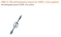
AND this is the light source for a i-line lithography system.
1644533874230.png
A course the are some complex electronics to power this Mercury lamp but gives an idea on how complex things becomes as features become smaller in a IC. It has become exponentially expensive.
 

9dashline

Captain
Registered Member
I meant it in a strategic way. Like oil is a strategic "weapon" which can be used to choke an economy to the ground, the same is for chips

A country without chips is a dead economy.
I am not against setting up chip foundries in Pakistan but my question is what would Pakistan offer to acquire such an extremely valuable thing.
Correct, but in the same way PC sales never replaced mainframe sales, they merely eclipsed them... same for smartphone vs desktop sales... Think of it as layers, everything in modern society relies ultimately on the energy/materials/infrastructure layer, once that layer is matured, then the value-add stuff comes into play... Although we are in the so-called digital age or 4th industrial revolution etc we haven't yet left the oil age... but making chips is predicated upon society having access to energy, materials and sufficient EROEI threshold... however "just" having oil is no longer enough to compete in this 21st century, and while oil /energy is the blood of modern civilization, so has computers/chips become equally as important... Just like a lot of the high earner jobs today (celebrities, VP, managers, etc) are because exists the foundation of lower 'real' jobs that prop it up and make the economies of scale possible for those fluffy jobs to exists in the first place, its only because the basics like food are already taken care of that society can afford to have jobs like chip engineers or software design etc etc...

We have not left the oil age, however as oil becomes more scarce, the US is already pivoting to holding semiconductor supply chain hostage (ASML, TSMC, etc etc) just like it held OPEC hostage with its military "protection" in exchange for forcing everyone to prop up the digital dollar (was the petrodollar) so that it can continue to tax, collect rent, and squeeze, sacrifice and cannablization the rest of the world to sustain its "nonnegotitable American Way of Life TM"
 

FairAndUnbiased

Brigadier
Registered Member
The most advanced working node is 90 nm, the 65 nm one is still in the development phase with some low-volume production -
Please, Log in or Register to view URLs content!
, scroll down and you will the asterisk which says "В разработке: проходит квалификацию и освоение в производстве". They do use ASML equipment also for older nodes - PAS 5500/750F (130 nm+) and PAS/1150C (90 nm+).

Are you sure? Russian Mikron bought both the tech process and equipment for 180 nm nodes back in 2006 from STMicro. Plus Russian
Please, Log in or Register to view URLs content!
uses ASML PAS 5500/250С for 350 nm production.
STMicro is a fab though so that's just buying their used equipment for 180 nm. The real value was their process, not the super depreciated equipment from the 90s.

I pointed out deposition, I don't think ASML produces any deposition equipment.
 

xypher

Senior Member
Registered Member
STMicro is a fab though so that's just buying their used equipment for 180 nm. The real value was their process, not the super depreciated equipment from the 90s.
It makes no sense that they would have the equipment for those processes but not the tech nodes themselves because all of that comes primarily from Soviet times, and Soviets for sure would not manufacture such equipment for third parties if they did not have the capability to utilize them on their own. Plus 350 nm is too advanced for the 80s. So, considering this, and the fact that another Russian institution utilizes an older ASML machine for 350 nm, I don't think there is an ability to produce machines for 180-350 nm nodes.

Moreover, Mikron acquired 90 nm process the same way - and they still utilize the bought equipment. Another example is Angstrom-T (which is now under revival process by their new owner NM-Tech who hired a bunch of Taiwanese specialists from UMC) fab bought equipment from GlobalFoundries for 90-130 nm nodes too. So clearly the value is not solely in the tech nodes but also in the equipment as well.
 

gelgoog

Lieutenant General
Registered Member
It makes no sense that they would have the equipment for those processes but not the tech nodes themselves because all of that comes primarily from Soviet times, and Soviets for sure would not manufacture such equipment for third parties if they did not have the capability to utilize them on their own. Plus 350 nm is too advanced for the 80s. So, considering this, and the fact that another Russian institution utilizes an older ASML machine for 350 nm, I don't think there is an ability to produce machines for 180-350 nm nodes.

Moreover, Mikron acquired 90 nm process the same way - and they still utilize the bought equipment. Another example is Angstrom-T (which is now under revival process by their new owner NM-Tech who hired a bunch of Taiwanese specialists from UMC) fab bought equipment from GlobalFoundries for 90-130 nm nodes too. So clearly the value is not solely in the tech nodes but also in the equipment as well.

Russia bought those tools and processes 2nd hand because it was much cheaper this way. Semiconductor fabrication is a really low priority in Russia. Even more so back then. Those fabs use 8 inch wafers. AFAIK Russia only has a single 12 inch (300mm) wafer fab. Crocus Nano Electronics. They are a memory manufacturer which manufactures MRAM. They collaborate with Chinese semiconductor company HLMC to develop their manufacturing process. HLMC is probably the 2nd best Chinese semi fab company after SMIC.

Russia had a Rusnano company called Mapper LLC working on the manufacture of MEMS e-beam hardware. This was being used basically as the write heads for e-beam lithography tools in development by Dutch company Mapper Lithography. Back when ASML bought Mapper Lithography they wanted to get Russian Mapper LLC but the Russian state stopped it. They weren't letting the Dutch get the technology Rusnano had spent millions investing on that easily.

That is likely the most sophisticated lithography technology Russia has access to. It is not a complete working tool. Russia uses imported lithography machines.

Russia is a world leader in sapphire crystal manufacture. These are used for all sorts of applications like LEDs and GaN.
Please, Log in or Register to view URLs content!
 
Last edited:

tokenanalyst

Brigadier
Registered Member
1644545897104.png

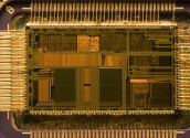
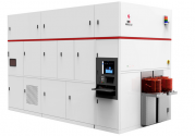
This is a 486DX2 processor made on an 800nm process and the die size is ~12mm x ~7mm, even with this old node the resolution of features on this thing is insane. The crazy thing is that this is the same resolution of the new SMEE packaging machine, from 800nm to 600nm, but this machine can theoretically pattern ~40 of them on a single 60mm x 60mm substrate. They're not kidding when they say "advanced packaging", this machine is for making really complex integrated circuit packages.

1644547111756.png
 
Status
Not open for further replies.
Top