Chinese semiconductor thread II

manqiangrexue

Brigadier
The US is allowing the H200 to be exported to China. Should China buy those chips. If you ask me China shouldn't buy the H200 and focus on her own chips and that is the govs view in China too. But can companies resist.

Isn't Nvidia already banned in China?
Please, Log in or Register to view URLs content!
"China set to limit access to Nvidia’s H200 chips despite Trump export approval"
Please, Log in or Register to view URLs content!
 

Hyper

Junior Member
Registered Member
BREAKING: China set to limit access to Nvidia’s H200 chips despite President Trump's export approval.

Buyers will likely be required to go through an approval process, submitting requests to purchase and explaining why domestic providers were unable to meet their needs.

Please, Log in or Register to view URLs content!
So many chips have been smuggled through Malaysia and Singapore.
 

tokenanalyst

Lieutenant General
Registered Member

Achieving A Breakthrough In The Localization Of High-Purity Precursor Materials.​


Hefei Andekeming Semiconductor Technology Co., Ltd. (Andecom) has achieved a major breakthrough in the independent development and production of high-purity thin-film deposition precursor materials—critical components in advanced semiconductor manufacturing. As global chip production shifts toward more sophisticated processes, these materials are essential for performance and reliability, yet long dominated by international firms.

Since its founding in 2018, Andecom has focused on domestic R&D and industrialization of advanced electronic-grade precursors. Recognized as a national-level "little giant" and high-tech enterprise, it has built strong research capabilities through a provincial technology center, innovation centers, and a world-class talent pool featuring overseas returnees and top-tier researchers. Over 30% of its workforce are dedicated to R&D, with multiple patents and international standard participation.

Andecom's strategic layout includes a "headquarters + bases + regional centers" model—centered in Hefei, with industrialization in Tongling and customer service hubs in Shanghai and Wuhan. In a key development, it is jointly investing with overseas industry leaders to build a high-purity precursor and electronic-grade solvent project in Hefei’s economic zone, expected to launch in 2027.

The company has posted extraordinary growth: CAGR over 100% for three years, explosive revenue expansion in 2025. It has developed more than 50 new products, filed 125 patents (81 inventions), and secured 33 invention patents. Andecom led one international standard and participated in two national standards.

Core Products:​

  1. La(iPr-fmd)₃ (Lanthanum-based High-K Precursor)
    • Independently developed with innovative purification technology (lithium salt substitution, crystallization sublimation).​
    • Achieves metal purity ≥99.9999%, impurities ≤50ppb, thermal stability up to 300°C.​
    • Used in atomic layer deposition (ALD) for advanced logic chips; performance at world-class level.​
    • Verified by China’s top chip foundry and DRAM makers; now the only domestic supplier with stable supply.​
  2. CpHf (Hafnium-based High-K Precursor)
    • Developed via "one-pot" synthesis and advanced purification.​
    • Achieves 6N metal purity, impurities ≤50ppb; superior to global leaders.​
    • Used in DRAM memory chips; high vapor pressure and thermal stability ensure performance.​
    • Mass-produced for major domestic DRAM and equipment firms; only domestic supplier for key clients.​
These products represent original advances in molecular design, synthesis, and purification backed by 35 patents (16 inventions)—and serve leading global and domestic semiconductor companies.​

Please, Log in or Register to view URLs content!
 

tokenanalyst

Lieutenant General
Registered Member

The second-generation vertical silicon carbide coating equipment of China Electronics Technology Group Corporation (CETC) has undergone process iteration and upgrade.​


Recently, the second-generation vertical silicon carbide coating equipment independently developed by CETC Equipment Shanxi CETC Co., Ltd. has successfully achieved a process technology upgrade, increasing furnace loading capacity by 70% and shortening the coating cycle by 33%.

Recently, the second-generation vertical silicon carbide coating equipment independently developed by CETC Equipment Shanxi CETC Co., Ltd. has successfully achieved a technological upgrade, increasing furnace loading capacity by 70% and shortening the coating cycle by 33%. The R&D team successfully overcame technical challenges such as flow field and temperature field uniformity control, coating process matching, and reducing by-products after more than 30 process experiments and structural design optimizations. Through continuous optimization of process parameters, the furnace loading capacity has been increased by 70% compared to the first-generation vertical silicon carbide coating equipment, while ensuring product performance. The coated products produced by this equipment fully meet the technical specifications, effectively satisfying the diversified and large-scale demands of the market.

Going forward, CETC Equipment Shanxi CETC Co., Ltd. will continue to focus on the field of semiconductor coating equipment, continuously improve its independent innovation and core technology capabilities, and contribute to the company's high-quality development.

Please, Log in or Register to view URLs content!
 

tokenanalyst

Lieutenant General
Registered Member

Xia Ning, Gallium Core Semiconductor: Large-size gallium oxide single crystal growth and defects​


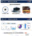
At the IFWS&SSLCHINA 2025 forum in Xiamen, Xia Ning, CTO of Hangzhou Gallium Core Semiconductor Co., presented a keynote on "Large-Size Gallium Oxide Single Crystal Growth and Defects." He highlighted advancements in growing high-quality gallium oxide (GaO) single crystals—key fourth-generation semiconductors with ultra-wide bandgap (4.8 eV), high breakdown electric field (8 MV/cm), UV transparency (>80%), and low manufacturing cost.
1765292409969.png

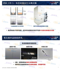
Key challenges include GaO's volatility at high temperatures, high melting point, and poor thermal conductivity, which complicate crystal growth and require specialized oxygen-rich environments and novel equipment. While methods like floating zone and cold crucible lack industrial viability, the Czochralski, casting, and vertical Bridgman (VB) techniques show strong potential especially casting and VB for large-scale production.
1765292438889.png

Gallium Core has successfully grown 8-inch GaO crystals in various orientations and doping levels using these methods. The technology enables high-quality, low-cost substrates, with projected costs under 2000 RMB per 8-inch wafer, expected to drop further within 2–3 years. This will help overcome industry bottlenecks such as large-area epitaxy, defect control, p-type doping, and high-current device fabrication.

With mass production on the horizon, GaO is poised to accelerate industrial adoption offering breakthroughs in defense and civilian applications (including power electronics, UV devices, and high-temperature systems) and drive a multi-billion dollar market.

Please, Log in or Register to view URLs content!
 

jx191

New Member
Registered Member
BREAKING: China set to limit access to Nvidia’s H200 chips despite President Trump's export approval.

Buyers will likely be required to go through an approval process, submitting requests to purchase and explaining why domestic providers were unable to meet their needs.

Please, Log in or Register to view URLs content!
This was always going to happen. If there is a domestic alternative, the govt won't allow you to indulge in Nvidia's offering. If you can prove that buying an H200 will support domestic development in some way, and there is no domestic alternative, you can buy some.

That's how I would see the conversation going between buyers and the govt.
 

sunnymaxi

Colonel
Registered Member
This was always going to happen. If there is a domestic alternative, the govt won't allow you to indulge in Nvidia's offering. If you can prove that buying an H200 will support domestic development in some way, and there is no domestic alternative, you can buy some.

That's how I would see the conversation going between buyers and the govt.
smuggling enough chips + domestic replacement is already available.. so Chinese firms literally don't need H200 in bulks.

anyways by 2027 China most likely will be self-sufficient in Ai chips. so US decision doesn't matter much.
 

jx191

New Member
Registered Member
smuggling enough chips + domestic replacement is already available.. so Chinese firms literally don't need H200 in bulks.

anyways by 2027 China most likely will be self-sufficient in Ai chips. so US decision doesn't matter much.
Yeah I saw a report by Morgan Stanley about how China's AI GPU share will be 50% domestic by 2027.

We know that Morgan Stanley is not a reliable source but it's interesting to see that even they are agreeing how China's AI domestic GPUs are expanding
 
Top