Chinese semiconductor thread II

tokenanalyst

Lieutenant General
Registered Member

Shanghai Silicon: 300mm silicon wafer capacity utilization rate is relatively high​


Shanghai Silicon Industry Group Co., Ltd. (688126.SH) released its Q3 2025 financial report, showing revenue of RMB 2.641 billion for the first three quarters (up 6.56% year-on-year) and a net loss of RMB 631 million; Q3 revenue was RMB 944 million (up 3.79% year-on-year) and a net loss of RMB 265 million. The main reasons for the losses include: sales of 300mm silicon wafers increased by over 30% but unit prices were under pressure; sales of 200mm silicon wafers decreased by about 10% and contract processing revenue dropped significantly; coupled with increased R&D investment (RMB 253 million in the first three quarters, up 21.63% year-on-year) and financial expenses from capacity expansion.On November 3rd, the company mentioned in an investor relations activity that the capacity utilization rate of 200mm silicon wafers has been slowly recovering due to sluggish application demand; the capacity utilization rate of 300mm silicon wafers is relatively high and sales are increasing, but prices are still under pressure due to domestic competition. Looking at the overall market, polished wafers for memory currently account for about 60-65% of the market, logic wafers about 30%, and the remainder are heavily doped power products. The company's market share is roughly the same.

Construction of Shanghai Silicon Production Line:

The Taiyuan project for upgrading the production capacity of 300mm silicon wafers for integrated circuits continues construction. The company's combined production capacity of 300mm semiconductor silicon wafers in Shanghai and Taiyuan has reached 750,000 wafers/month. The combined production capacity of polished wafers and epitaxial wafers of 200mm and below from subsidiaries Xin'ao Technology and Okmetic exceeds 500,000 wafers/month. The combined production capacity of SOI silicon wafers of 200mm and below from subsidiaries Xin'ao Technology and Okmetic exceeds 65,000 wafers/month. The current production capacity of 300mm SOI silicon wafers from subsidiary Xin'ao Core is approximately 80,000 wafers/year, and it is expected to continue to increase the production capacity to 160,000 wafers/year this year. Subsidiary Jinke Silicon Materials has successively obtained system certifications from multiple customers. The Taiyuan factory continues to promote the certification of 300mm products and has now completed the quality system audits of multiple customers, gradually starting to realize the mass sales of positive wafers.

Please, Log in or Register to view URLs content!
 
Last edited:

tokenanalyst

Lieutenant General
Registered Member

Lithography company SVG Optronics wants to expand into the IC lithography market.​

Suzhou Vigor (SVG Optronics) acquired a 51% stake in Changzhou Weipu (VPTEK) for 510 million yuan, expanding its presence in the semiconductor defect detection equipment field.​


Suzhou Vigon announced that it plans to acquire a 51% stake in Changzhou Weipu Semiconductor Equipment Co., Ltd. (hereinafter referred to as "Changzhou Weipu") for RMB 510 million using its own or self-raised funds. After the transaction is completed, Changzhou Weipu will become a holding subsidiary of Suzhou Vigon and will be included in the consolidated financial statements.

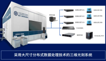
In its announcement, Suzhou Vigor stated that the acquisition will allow both parties to leverage their respective strengths in laser direct-write lithography and mask defect detection. Firstly, the company can utilize Changzhou VIP's customer resources and mass production experience to accelerate the mass production application of laser direct-write lithography machines in semiconductor photomask manufacturing and advanced packaging. Secondly, the company can assist Changzhou VIP in its development of advanced process optical systems.
1762531604512.png
1762531209294.png

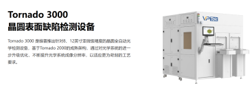
Changzhou Weipu was established in March 2019 with a registered capital of 3.4663 million yuan. Its main business is the research, development, production and sales of photomask defect detection equipment and wafer defect detection equipment. Both types of products are core equipment for semiconductor quality inspection.

Please, Log in or Register to view URLs content!
 

tokenanalyst

Lieutenant General
Registered Member

深圳平湖实验室 has unveiled GaN MPW (Multi Project Wafer) service that allows each 8-inch GaN wafer to test multiple designs over 25mm2 units/"shots". Paired with its GaN PDK to design, fab & cut/test dies so they can be taped out & validated. 650V MPW becomes available in 2025Q4 & 100V MPW in 2026Q1
Interesting for small companies and startups.
 

tphuang

General
Staff member
Super Moderator
VIP Professional
Registered Member
Interesting for small companies and startups.
yep, GaN chip designers in China have quite the advantage.

Please, Log in or Register to view URLs content!

looks like SMIC is buying out the Beijing gov't controlled portion of SMIC North. This has 70k wpm of 12-inch capacity. Producing mostly 40 and 28nm chips.

It is kind of obvious by now that initial funding is more like loans in a way so that fabs can have the capital needed to build their fabs. Once they have the cash, they will buy back the remaining shares
 

tokenanalyst

Lieutenant General
Registered Member

Founder Technology plans to invest 1.364 billion yuan to expand production and strengthen its position in the high-end AI PCB market.​

Founder Technology issued an announcement stating that it will invest 1.364 billion yuan to build an artificial intelligence expansion project at its Chongqing production base in order to break through the bottleneck of high-end product capacity and seize the explosive growth in market demand.

Founder Technology points out that against the backdrop of the rapid development of next-generation information technology globally, the PCB industry has entered an era of technological innovation represented by artificial intelligence. The demand for high-end PCBs with high data capacity, high density, high speed, low loss, and high reliability is becoming increasingly urgent for equipment such as high-speed switches, AI servers, storage, and 5G macro base stations. In particular, the widespread adoption of 400G, 800G, and even 1.6T high-end switches and next-generation servers has driven explosive growth in the market for related core components.

Founder Technology's wholly-owned subsidiary, Chongqing Gaomi, is a company specializing in the research and development and manufacturing of high-frequency, high-speed, and high-density interconnect printed circuit boards. Its products, featuring leading technological characteristics, are widely used in high-end switches, servers, and storage devices in the field of artificial intelligence. However, the company admits that its existing production capacity in Chongqing is insufficient to meet the continuous demand from customers, and this capacity bottleneck has become a key factor restricting the company's development.

Please, Log in or Register to view URLs content!
 

tokenanalyst

Lieutenant General
Registered Member
From the surface for LPP space we have:

At least two companies developing MOPA CO2 Lasers.
At few developing ultra low thermal expansion materials for collectors mirrors.
Another developing giant Ion figuring machines
At few for multilayer mirrors coating
This one looks like is making Tin droplet generators for EUV sources.
Photoresist standards, that means companies
SMEE EUV Metrology
A few racing to built EUV mask metrology tools.
A few ones developing EUV sensing technology.
The past year the development of the giant chambers for mirrors metrology that most stooges post the pic about it has already being develop.
At least a few for EUV-Vibration damping technology
U-Precision MagLev Wafer Stages.
A few for high end vacuum for EUV.

Most of those technologies are compatible with LDP.
more than half are compatible with DPP.
And more than half with FEL-EUV and SSMB.

My guess is that for each EUV company that we post here there should be at least 3 or 5 that we don't anything about it and multiple developing technologies to support those ones. For example a ceramic company making ultra high end parts for these companies. A gigantic EUV supply network is brewing inside China.
<I. Technological Revolution in Domestic Lithography Machines

China's domestically produced lithography machines, employing laser-induced discharge plasma (LDP) technology, are expected to enter trial production in the third quarter of 2025. Featuring a compact design and a 40% reduction in energy consumption, this marks a significant step towards true self-reliance in the most cutting-edge semiconductor manufacturing field. This breakthrough may alter the traditional chip industry chain structure of "design abroad, manufacturing in East Asia, and application in China."

ASML, a traditional lithography machine giant, uses laser-induced plasma (LPP) technology in its EUV lithography machines. This technology relies on expensive and complex high-energy lasers to bombard tin droplets to generate plasma, and its control system is based on a precision FPGA. In contrast, the core of China's LDP technology lies in vaporizing the tin material between the electrodes and then converting it into a plasma state through high-voltage discharge. This "directional explosion" approach may be simpler and more efficient.

The Hyperion-1 prototype exhibits exciting features, such as a design that is one-third the size of ASML's, significantly reduced power consumption, and a clear manufacturing cost advantage. Although its power consumption is lower (50W vs. ASML's 250W), it has already achieved small-batch production of 5-3 nanometer nodes. Currently, its production capacity is approximately 10 wafers per hour, focusing on R&D and X-series chips. The plan is to launch Hyperion-2 by 2026, increasing production capacity to 150W/hour and achieving commercial production.>


Please, Log in or Register to view URLs content!
----------------
I know that post is controversial, but I think there are already EUV pilot lines in China, that is not just a EUV research lab, EUV pilot lines, a step closer to production, of course I think that the current systems are not even close to ASML, probably a few dozens wafers per hour like the post says, but the goal of 80 or even 100 wafers per hour by 2027 is a very high probability.
I think people inside this development in China already know where things are going and institutions and their companies are RUSHING to be first in the commercialization of EUV. I think, that most traditional supplier of lithography sub-systems like RS-Laser and Guowang Optical are now focus on KrF, ArF and ArFi, so they have to move fast.
 
Top