Chinese semiconductor thread II

tokenanalyst

Lieutenant General
Registered Member
so this seems like same product line as 领聚科技's product from earlier this thread.

Any idea if there are other Chinese companies in this field? And also how competitive this is to the Lingju product?
From my point of view in the high semiconductor end, looks like is: Raiven, Tsinghua U-Precision and Harbin Lingju Technology with the oldest of the three being U-precision.

There also more companies that could fill the gaps in low to middle end lithography, semiconductor metrology, advance packaging and numerical machining.

China precision measurement companies, for semiconductors and other industrial applications.

Chotest:


View attachment 162945
With more than 15 years of professional technology accumulation, we designed and manufactured White Light Interferometer SuperView W1, Laser Tracker GT series, Universal Thread Measuring Machines SJ5200 series, Universal Length Measuring Machines SJ5100 series, Laser Interferometer SJ6000, Profilometers SJ5700 series, Automated Dial Indicator Testing Machines SJ2000 series and other high-end measuring equipment. We provide high precision measurement solution from nanometer to hundred meters.

Please, Log in or Register to view URLs content!

Shanghai Paipin:

Shanghai Pai-pin Optic-Electric Technology Co., Ltd. specializes in dual frequency laser interferometry technology research and product development. Our services serve the semiconductor equipment, ultra-precision motion control, length metrology, precision machine tool calibration, vibration, velocity, and acceleration testing industries.

Our core team is composed of professionals in optics, mechanics, electronics, sales, etc., with more than ten years of experience in dual-frequency laser interferometer product development and its application. We are one of the dual-frequency laser interferometer teams with the most extensive engineering experience in China.


View attachment 162946
Please, Log in or Register to view URLs content!

Tsinghua U-Precision:
Beijing Huazhuo Jingke Technology Co., Ltd. was established on May 9, 2012. It is a national high-tech enterprise. Its main business is to research, develop and produce ultra-precision measurement and control equipment components and ultra-precision measurement and control equipment complete machines based on ultra-precision measurement and control technology, and provide related technology development services.

View attachment 162955

Please, Log in or Register to view URLs content!

Beijing Leice:

Beijing Leice Technology Co. Ltd., originated from Sate Key Laboratory of Precision Measurement Technology Instruments, Tsinghua University, is a high-tech company that offers measurement solutions as well as precision laser measurement instruments with independent intellectual property rights.Leice offers dual-frequency laser interferometer, laser feedback interferometer, phase retardation measurement instrument, laser teaching instrument, and laser nanometer ruler, etc. It can meet the demand for precision measurement of mechanical manufacturing, microelectronics, optical manufacturing, scientific research and education industries, etc.

View attachment 162956

Please, Log in or Register to view URLs content!

And others
 

CMP

Captain
Registered Member
To be honest, with the abject failure of mmwave 5G, terahertz 6G is a pipe dream. 5G mmwave is a complete failure at this point. Vendors have trialed mmwave equipment but hardly any commercial deployment. Very few deployments.
IIRC the main reason is because mmwave has very poor coverage. Just as a function of the fundamental physics at play, even a thin solid surface can block the signal.
 

tokenanalyst

Lieutenant General
Registered Member

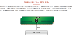
Montage Technology successfully mass-produced DDR5 fourth-generation RCD chips​


Montage Technology announced the successful mass production of its DDR5 fourth-generation Register Clock Driver (RCD04) chip, a key component in high-performance server and data center memory systems. The RCD04 offers improved transmission speed, energy efficiency, and signal integrity, supporting higher bandwidth and lower power consumption making it ideal for AI computing, big data analytics, and cloud platforms.
1761769862920.png

This achievement underscores Montage’s technological leadership in the global memory interface chip market and strengthens its product portfolio in the DDR5 era. As a leading domestic designer of memory interface and signal enhancement chips, Montage plays a vital role in advancing domestic server and data center capabilities.

In the first half of 2025, the company reported operating revenue of RMB 2.633 billion (up 58.17% year-on-year) and net profit of RMB 1.159 billion (up 95.41%), significantly exceeding market expectations. Driven by innovation and strong demand, the company has proposed a cash dividend of RMB 2 per 10 shares (totaling RMB 227 million inclusive of tax), reflecting its commitment to shareholder value.

The performance growth highlights Montage’s strong market position and sustainable development momentum. Looking ahead, the company plans to further boost R&D investment, expand applications in high-performance computing, and maintain a focus on delivering long-term value to investors.

Please, Log in or Register to view URLs content!
 

tokenanalyst

Lieutenant General
Registered Member

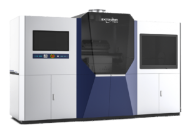
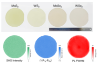
Jimoxin Technology and Nanjing University are featured in Science! Breakthrough in key technology for preparing two-dimensional semiconductor single crystals​


Nanjing Extreme Molybdenum Core Technology Co., Ltd. (hereinafter referred to as " Extreme Molybdenum Core Technology ") and a research team from Nanjing University jointly published important research results in the journal *Science*. Extreme Molybdenum Core Technology was deeply involved in process development and equipment manufacturing , providing the research team with its independently developed two-dimensional semiconductor MOCVD equipment, the Oxy-MOCVD 200 ultra , successfully achieving the world's first mass production of 6-inch two-dimensional semiconductor single crystals. The complete localization and independent controllability of this equipment marks a significant breakthrough for China in the field of key materials and equipment for next-generation integrated circuits . Extreme Molybdenum Core Technology simultaneously launched several two-dimensional semiconductor single crystal wafers and single crystal substrates, providing high-quality material solutions for scientific research and industrial applications.

1761770410566.png

Technological Breakthrough: Achieving Synergistic Innovation of Mass-Production Performance and Flexible Processes

The MOCVD equipment from Jimo Core Technology is an original design based on fundamental principles, possessing a high degree of professionalism and process adaptability, providing a reliable mass-production-grade technology platform for the growth of two-dimensional semiconductor single crystals. The core of this breakthrough lies in the successful integration of research-grade process flexibility with mass-production-grade process stability. Compared to the limitations in controllability and uniformity of traditional fabrication techniques, the newly developed technology demonstrates significant advantages in large-size wafer uniformity and process stability. This equipment integrates several independently developed core technologies:

1. The “Precise-Flow” precursor transport system enables precise control and long-term stability of gas flow rate, ensuring consistent material quality.

2. The “Multi-Zone Thermal” temperature field control module supports the precise execution of complex temperature curves, providing an ideal environment for the development of diverse processes;

3. Open process architecture, allowing users to flexibly adjust process parameters according to R&D needs, achieving controllable growth throughout the entire process from material nucleation to wafer scaling.

1761770445819.png

Please, Log in or Register to view URLs content!
 

Wahid145

Junior Member
Registered Member
I have notice that Naura has quietly been adding semiconductor tools to their catalog.

The Landscape: A plasma etching-doping system that implant Ions into junctions and trenches of ICs, different from Ion implanters that accelerate particles using magnets this looks likes use energy of the plasma field to implant the atoms. The equivalent would be AMAT VIISta

View attachment 163562
The ACCURA Family: already discuss here, for deep hole-trench, dielectric etching and 3D-NAND
View attachment 163563
The Surefill W Family: For Tungsten thin film Chemical Deposition for the interconnects in ICs, my guess is to compete with AMAT Endura, especially with AMEC Preforma Uniflex.

View attachment 163564

They Also entered the Ion Implantation business, the Sirius family and the Rapid Thermal Processing business with the Sitara family probably to complement their Ion Implanters, RPT tools are used after Ion Implantation basically recrystallize the atoms after doping.
View attachment 163566
I don't have a lot of knowledge on this, but do you think you can make an excel file or a summery as to all the AMAT equivalent from Naura, AMEC and Piotech? Am wondering about the AMAT/LAM replacement for a very long time now.

And ya, when I checked Naura website few years ago, there were only a handful of deposition tools and almost all of them were for 8in wafers. Now so many more almost out of nowhere. I wonder which Deposition tools are missing at this point which only AMAT has.
Still can't believe AMAT/LAM are having 30%+ sales revenue from China...
 

tokenanalyst

Lieutenant General
Registered Member
I don't have a lot of knowledge on this, but do you think you can make an excel file or a summery as to all the AMAT equivalent from Naura, AMEC and Piotech? Am wondering about the AMAT/LAM replacement for a very long time now.
That could be interesting from a historical record point of view.
And ya, when I checked Naura website few years ago, there were only a handful of deposition tools and almost all of them were for 8in wafers. Now so many more almost out of nowhere. I wonder which Deposition tools are missing at this point which only AMAT has.
Still can't believe AMAT/LAM are having 30%+ sales revenue from China...
Their competition is heating up, I think they would rather have a level of secrecy about their tools but if AMEC, Piotech and other are going to brag about similar or more advanced tools that doesn't help them to increase their market valuation.
One of the reason for the secrecy in lithography is because none of the companies involved are public.
 

Jilternj

Just Hatched
Registered Member
I don't have a lot of knowledge on this, but do you think you can make an excel file or a summery as to all the AMAT equivalent from Naura, AMEC and Piotech? Am wondering about the AMAT/LAM replacement for a very long time now.

And ya, when I checked Naura website few years ago, there were only a handful of deposition tools and almost all of them were for 8in wafers. Now so many more almost out of nowhere. I wonder which Deposition tools are missing at this point which only AMAT has.
Still can't believe AMAT/LAM are having 30%+ sales revenue from China...
but what will be more interesting is that if amat/lam has 30+ sales from china, and we know there are naura, amec also sells some of theirs in China , and rapidly inscresasing, so what means the FAB capacity added will be much more than 30% in China, in the coming years, the fab capacity will be like real over-capacity for the world.
 

tokenanalyst

Lieutenant General
Registered Member
but what will be more interesting is that if amat/lam has 30+ sales from china, and we know there are naura, amec also sells some of theirs in China , and rapidly inscresasing, so what means the FAB capacity added will be much more than 30% in China, in the coming years, the fab capacity will be like real over-capacity for the world.
In the next years the next logic nodes to expand capacity in China are going to be 14nm->7nm->5nm-3nm there are still years of room for capacity on those nodes. Also DRAM and NAND there still years of room of capacity there. That no even counting capacity in MEMs and Photonics. Also the final goal is to basically to replace US made tools and chips for domestics ones giving that the trust that US will fulfill its commercial obligations is gone.
 

tphuang

General
Staff member
Super Moderator
VIP Professional
Registered Member
Please, Log in or Register to view URLs content!

united Nova got 500m RMB bond issuance. Good to see for them since they got issued at just 1.6% yield and this will significantly lower their capital. I think it helped here that they became profitable. They are a major core part of China's auto, NEV, industrial and consumer electronics supply chain for MEMS, IGBT, MOSFET, analog and MCUs.
 

tokenanalyst

Lieutenant General
Registered Member

Jingsheng Mechanical & Electrical disclosed the latest progress on silicon carbide production capacity and semiconductor equipment orders.​


Recently, Jingsheng Mechanical & Electrical received research from multiple institutions, and disclosed information about the company's silicon carbide production capacity layout and semiconductor equipment orders.

Jingsheng Mechanical & Electrical pointed out that the company is actively expanding its silicon carbide production capacity, with a project in Shangyu to produce 300,000 silicon carbide substrates per year; and based on the good development prospects and broad market of the global silicon carbide industry, it is building an 8-inch silicon carbide substrate industrialization project in Penang, Malaysia, to further strengthen the company's supply capabilities in the global market; at the same time, it is building a supporting crystal project in Yinchuan with an annual production capacity of 600,000 8-inch silicon carbide substrates, continuously strengthening the company's technological and scale advantages in the field of silicon carbide substrate materials.

Meanwhile, Jingsheng Mechanical & Electrical introduced that its subsidiary, Zhejiang Jingrui SuperSiC, has established a 12-inch silicon carbide substrate pilot line that covers the entire process of crystal processing, cutting, thinning, chamfering, grinding, polishing, cleaning, and testing. All processes utilize domestically produced equipment and proprietary technologies. Core processing equipment such as high-precision thinning machines, chamfering machines, and double-sided precision grinding machines were developed and refined by the company over many years, achieving industry-leading performance. With the official copper wire connection of this pilot line, Jingsheng Mechanical & Electrical has formally formed a complete closed loop for 12-inch SiC substrates, from equipment to materials, completely resolving the "bottleneck" risk of key equipment and providing a new benchmark for cost and efficiency for downstream industries.

Please, Log in or Register to view URLs content!
 
Top