Chinese semiconductor thread II

tokenanalyst

Lieutenant General
Registered Member

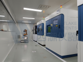
West Lake Instruments Product Demonstration Center was completed and put into trial operation​


Recently, Westlake Instruments (Hangzhou) Technology Co., Ltd. announced that its product demonstration center has been completed and put into trial operation.
1761670600749.png

The center is a comprehensive platform integrating an 8-inch SiC laser lift-off automated production line and large-scale SiC substrate processing verification. With the ability to verify cutting-edge technologies and products, it is a key vehicle for advancing laser lift-off technology from "process feasibility" to "mass production usability." This combination of "mass production demonstration" and "cutting-edge verification" enables the center to provide customers with comprehensive support from process introduction to mass production decision-making.

As the core of the product demonstration center, the 8-inch SiC laser lift-off automated production line achieves full automation and unmanned operation from ingot to wafer, making it a powerful industrial tool for meeting current market demands and achieving cost reduction and efficiency improvement. The verification line produces over 20,000 8-inch substrates annually. Its modular design allows for flexible capacity allocation and provides customers with comprehensive, multi-level verification data.

The large-scale SiC laser lift-off process verification line primarily serves new technology and product validation for 12-inch SiC substrates. With an annual production capacity of over 10,000 12-inch substrates, it can also meet the processing needs of various non-standard large-scale seed crystals. Its core mission is to overcome large-scale process challenges, conduct forward-looking technological research and development, and provide technical reserves and solutions for the next generation of large-scale substrate processing.

Please, Log in or Register to view URLs content!
 

tokenanalyst

Lieutenant General
Registered Member

GaN terahertz technology breakthrough​


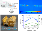
The Nanjing Institute of Electronic Devices (NIEID) has achieved a major breakthrough in terahertz technology by developing a high-performance 340 GHz frequency multiplier chain using gallium nitride (GaN) monolithic integrated circuit technology. Published in Infrared Physics and Technology, the study, led by Drs. Zheng Yiyuan and Zhang Kai, addresses the long-standing challenge of low output power in terahertz solid-state sources.

Terahertz waves offer wide bandwidth, strong penetration, high security, and good directionality—making them vital for ultra-high-speed communications, imaging, and sensing. However, generating powerful signals at 340 GHz has been hindered by material limitations and thermal issues. GaN’s superior power handling and thermal properties make it ideal for this application.

The new design combines a multi-anode GaN Schottky barrier diode (SBD) array with a high-thermal-conductivity silicon carbide (SiC) substrate, enhancing heat dissipation and power tolerance. A novel bias circuit optimizes SBD operation to improve frequency-doubling efficiency.

Experimental results show record-breaking continuous-wave output powers: 411 mW at 170 GHz, 82.2 mW at 340 GHz, and over 50 mW across the 320–350 GHz range—the highest reported globally. This breakthrough enables efficient, high-power terahertz generation and opens new possibilities for next-generation wireless communications, imaging, and remote sensing technologies.
1761689387687.png

Please, Log in or Register to view URLs content!
 

tphuang

General
Staff member
Super Moderator
VIP Professional
Registered Member

GaN terahertz technology breakthrough​


The Nanjing Institute of Electronic Devices (NIEID) has achieved a major breakthrough in terahertz technology by developing a high-performance 340 GHz frequency multiplier chain using gallium nitride (GaN) monolithic integrated circuit technology. Published in Infrared Physics and Technology, the study, led by Drs. Zheng Yiyuan and Zhang Kai, addresses the long-standing challenge of low output power in terahertz solid-state sources.

Terahertz waves offer wide bandwidth, strong penetration, high security, and good directionality—making them vital for ultra-high-speed communications, imaging, and sensing. However, generating powerful signals at 340 GHz has been hindered by material limitations and thermal issues. GaN’s superior power handling and thermal properties make it ideal for this application.

The new design combines a multi-anode GaN Schottky barrier diode (SBD) array with a high-thermal-conductivity silicon carbide (SiC) substrate, enhancing heat dissipation and power tolerance. A novel bias circuit optimizes SBD operation to improve frequency-doubling efficiency.

Experimental results show record-breaking continuous-wave output powers: 411 mW at 170 GHz, 82.2 mW at 340 GHz, and over 50 mW across the 320–350 GHz range—the highest reported globally. This breakthrough enables efficient, high-power terahertz generation and opens new possibilities for next-generation wireless communications, imaging, and remote sensing technologies.
View attachment 163527

Please, Log in or Register to view URLs content!
unbelievable. the power at these range for long range sensing is unbelievable, IIRC, there should be very little atmospheric attenuation at 170 GHz. So if they want to do 6G LEO constellation data transmission. Or in the future. satellite based early warning system. This works out pretty well.

And curious they were able to achieve this level of power with SiC substrate, that they didn't need diamond film layer or something.
 

gpt

Junior Member
Registered Member
Please, Log in or Register to view URLs content!

Impact of coherent wiggler radiation impedance in Tau-Charm factories​

Coherent synchrotron radiation (CSR) has long been recognized as a significant source of longitudinal impedance driving microwave instability in electron storage rings. In the pursuit of higher luminosity, next-generation circular +⁢− colliders operating in the few-GeV energy range, such as B-factories and Tau-Charm factories, are being designed with low-emittance beams and high beam currents. Damping wigglers are commonly introduced to reduce damping times and control beam emittance. In this study, we systematically investigate the impact of coherent wiggler radiation (CWR), a specific form of CSR generated within wigglers, on beam stability in Tau-Charm factories. We revisit the threshold conditions for CWR-induced microwave instability and evaluate its effects under realistic lattice configurations of collider rings. Furthermore, we examine theoretical models of longitudinal CWR impedance and identify improved formulations that better capture its influence. As an illustrative example, the developed CWR impedance models are applied to simulate beam stability in the Super Tau-Charm Facility currently under design in China.

Simpler explanation is as the electron bunch passes through a wiggler, it emits CWR. This process isn't frictionless. The emission creates an electromagnetic drag (a recoil force) that acts back on the bunch. This drag results in a net energy loss for the beam and it can disrupt the delicate energy balance needed for SSMB operations.

Impedance is the mathematical description of the drag force, the ratio of the wakefield voltage to the beam current. So this research is trying to quantify this drag to find ways to counteract it, either by modifying the ring design or by suppressing the radiation itself.
 

PopularScience

Senior Member
Registered Member
Please, Log in or Register to view URLs content!

Two major technological breakthroughs highlighted in AMEC's third-quarter report: mass production of high-end etching machines for memory chips and the achievement of internationally advanced performance levels for multiple thin-film equipment.

The next-generation 90:1 ultra-high aspect ratio dielectric etching equipment is about to enter the market.
 

tokenanalyst

Lieutenant General
Registered Member

The Ministry of Industry and Information Technology reported that China's integrated circuit output reached 381.9 billion units in the first three quarters, a year-on-year increase of 8.6%.​


The Ministry of Industry and Information Technology (MIIT) released data on the operation of the electronic information manufacturing industry in the first three quarters of 2025. In the first three quarters, the added value of the electronic information manufacturing industry above designated size increased by 10.9% year-on-year, 4.7 and 1.3 percentage points higher than the growth rates of the overall industrial sector and high-tech manufacturing sector, respectively. In September, the added value of the electronic information manufacturing industry above designated size increased by 11.3% year-on-year.

Among the main products, mobile phone production reached 1.11 billion units, a year-on-year decrease of 4.8%, of which smartphone production reached 881 million units, a year-on-year increase of 1%; microcomputer equipment production reached 251 million units, remaining flat year-on-year; and integrated circuit production reached 381.9 billion units, a year-on-year increase of 8.6%.

Please, Log in or Register to view URLs content!
 
Top