News on China's scientific and technological development.

AssassinsMace

Lieutenant General

After Fukushima, Europe decided to turn away from nuclear power plants and for some reason they expected China to follow suit yet the West expects China to reduce its carbon footprint which turning away from nuclear power generation won't do. So how do they expect China to achieve a zero carbon footprint? Oh yes China has to end all industrial activity eliminating China as a competitor to the West. How convenient. Now is Europe thinking about keeping their nuclear power plants running longer since they've lost a major source of where they get natural gas? And they wanted China to stop using nuclear power just because that's what they're doing.

Notice how everything China puts a lot of effort into is interpreted by the West as China is trying to dominate the world in that field? Even with Made in China 2025 where China seeks to end dependency on the West it's interpreted as China trying to dominate the world. Western countries are seeking to end foreign dependency and that's seen as a national security issue therefore their right. But not China's right. Look at rare earths. Most rare earths can be found everywhere. China doesn't monopolize access to it. The West is just a bunch of cheap bastards where they're not willing to pay the costs associated in producing concentrated rare earth elements on the own. Their dilemma of being dependent on China is their own fault. China is not preventing them from getting rare earth ores nor is preventing them from processing and refining it themselves. So like nuclear power plants, what are they suggesting China do to make them at ease? Of course the only way to make them feel comfortable is China has to surrender to the West where they're in control where they get to decide who gets China's production of rare earths. It's not like it was before that everyone had a equal share of the pie. It was the US and the West dominating all these areas and they conveniently saw no problem with that. Now dominating is wrong when the West isn't the one doing the dominating.

It's just like Trump blaming China when he outsources to China to buy his furnishings for the buildings he constructs and produce his signature products. He says he would be buying American if it weren't for China offering less expensive alternatives. No, he can still buy American. He's just a greedy SOB trying save as much money for himself. Just because there's a less expensive alternative, it doesn't mean he has to buy it. He made the choice, not China. Just like there's nothing preventing the US from producing rare earths themselves except their own greed because everything the US does cost more money to do. China has nothing to do with it. But those lame excuses work in the US because Americans are taught to spurn anything that makes it look it the US's own fault so blaming foreigners is the next best option.
 

Strangelove

Colonel
Registered Member
BeiDou x HSR x 5G x IoTs x data...


Please, Log in or Register to view URLs content!

China's BeiDou railway project passes acceptance review

Technology 18:15, 20-Mar-2022
a810648bca744a7e9435bff6fe628477.jpeg


The comprehensive application demonstration project of the BeiDou railway industry passed acceptance review on Thursday, effectively promoting the deep integration of China's BeiDou Navigation Satellite System (BDS) and high-speed railway system, China Media Group reported on Sunday.

Integrating big data, Internet of Things, 5G and cloud computing, the project has promoted over 8,000 sets of BeiDou terminal equipment in railway business sectors such as railroad engineering survey, automatic monitoring system, and high-speed train control system.

The project has also been extended and applied in fields such as integration of transportation and travel, and positioning and tracking of railway beams and emergency repairs.

China's BDS has entered a new phase of sustained stable services and rapid development, according to the China Satellite Navigation Office on March 11.

Measured by the global continuous monitoring and evaluation system, the BDS-3 system shows an advanced performance index in providing global positioning, navigation and timing services, with more outstanding performance in the Asia-Pacific region, said the office.

As planned, the BDS project will launch new satellites, further enhance the system stability and reliability, and conduct new-tech experiment and verification to ensure the continuous upgrading of the system, the office added.
 

KYli

Brigadier
Please, Log in or Register to view URLs content!

(ECNS) -- China's first Beidou positioning system for subways began construction on the Beijing Subway Capital Airport Express line Sunday.


The largest indoor space navigation and positioning system in China is expected to be finished within this year.


This project will cover a 30-kilometer-long section of the Beijing Subway Capital Airport Express and five stations on this line.


The BeiDou Navigation Satellite System (BDS), an essential space infrastructure of China, will provide services that include positioning, navigation and timing.


However, in some spaces where satellite signals are blocked and cannot be used, such as underground, underwater or in buildings, positioning and navigation need further improvement.


"We will combine indoor and outdoor positioning in subways, that is, Beidou and its augmented reality technology will be used outdoors to achieve high-accuracy positioning, and indoor positioning technology integrated with 5G will be used to allow users to receive indoor positioning signals," said Lin Luzhou, vice president of GNSS and LBS Association of China.


The system will improve the positioning accuracy in subways to less than two meters, making it available for vehicle dispatching, passenger transport organization, and emergency response.


In addition, it allows passengers to use their phones to navigate and position in complex environments in subway stations through three-dimensional navigation.
 

tokenanalyst

Brigadier
Registered Member

Research progress of femtosecond laser direct writing of 3D inorganic nanostructures​


In recent years, the precise and controllable preparation technology of three-dimensional (3D) inorganic nanostructures has become a research hotspot and plays an important role in the fields of aerospace, microelectronic devices, quantum chips, solar cells and structural materials. Inorganic material precursors are easy to crystallize, which makes it difficult to directly prepare 3D inorganic micro-nano structures at one time. Laser 3D printing technology is one of the important means to prepare three-dimensional inorganic microstructures. However, when preparing inorganic microstructures, its feature size and processing resolution are limited by materials and optical diffraction limits, making it difficult to achieve nanoscale preparation. The miniaturization, integration and 3D stereoization of devices have put forward higher and higher requirements for the feature size of 3D inorganic nanostructures. The development of superdiffractive 3D nanolithography technology and the preparation of 3D inorganic structures with nanometer feature size have become an urgent problem to be solved. The problem.

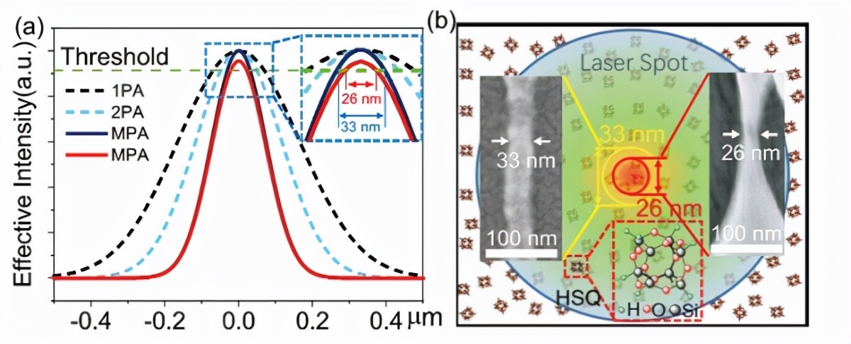
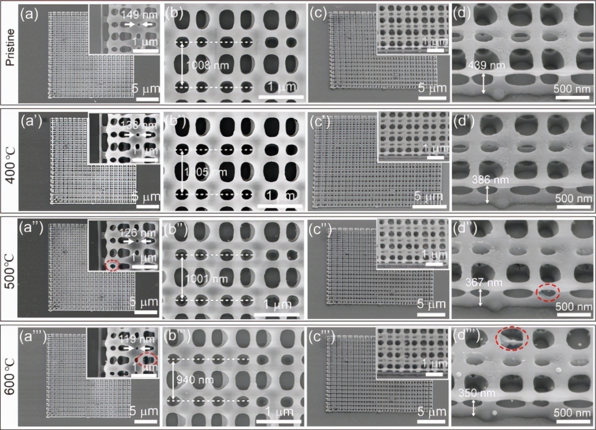
  Recently, the team of Zheng Meiling, a researcher at the Organic Nanophotonics Laboratory of the Biomimetic Intelligent Interface Science Center of the Institute of Physical and Chemical Technology, Chinese Academy of Sciences, and the team of Professor Duan Xuanming of Jinan University have made new achievements in the preparation of 3D inorganic nanostructures by femtosecond laser superdiffraction nanolithography. progress. The scientific research team used a femtosecond laser with a wavelength of 780 nm (repetition frequency of 80 MHz, pulse width of 120 fs) as a light source to break through the limitation of the optical diffraction limit and obtained an inorganic photoresist HSQ (hydrogen silsesquioxane). In order to achieve a 26 nm lithographic feature size that is only one-thirtieth of the laser wavelength (λ/30), 3D inorganic microstructures with excellent high temperature and solvent resistance were fabricated. In addition, the research also used femtosecond laser superdiffraction nanolithography to construct a variety of photonics microdevices and biomimetic microstructures based on inorganic nanostructures. The related research results were published in Nature Communications under the title of λ/30 Inorganic Features Achieved by Multi-Photon 3D Lithography .

the research work is supported by the National Key R&D Program "Nanotechnology", the National Natural Science Foundation of China, the Natural Science Foundation of Beijing Municipality, and the International Partnership Program of the Chinese Academy of Sciences.


Research progress of femtosecond laser direct writing of 3D inorganic nanostructures


Figure 1. Schematic diagram of light field distribution of femtosecond laser direct writing of inorganic nanostructures

Research progress of femtosecond laser direct writing of 3D inorganic nanostructures


Figure 2. Thermal resistance study of the 3D HSQ bilayer line array structure by femtosecond laser direct writing


Research progress of femtosecond laser direct writing of 3D inorganic nanostructures


Figure 3. HSQ bilayer array structure with heat resistance and biomimetic structural color by femtosecond laser direct writing

Please, Log in or Register to view URLs content!
 

Quickie

Colonel
Research progress of femtosecond laser direct writing of 3D inorganic nanostructures

In recent years, the precise and controllable preparation technology of three-dimensional (3D) inorganic nanostructures has become a research hotspot and plays an important role in the fields of aerospace, microelectronic devices, quantum chips, solar cells and structural materials. Inorganic material precursors are easy to crystallize, which makes it difficult to directly prepare 3D inorganic micro-nano structures at one time. Laser 3D printing technology is one of the important means to prepare three-dimensional inorganic microstructures. However, when preparing inorganic microstructures, its feature size and processing resolution are limited by materials and optical diffraction limits, making it difficult to achieve nanoscale preparation. The miniaturization, integration and 3D stereoization of devices have put forward higher and higher requirements for the feature size of 3D inorganic nanostructures. The development of superdiffractive 3D nanolithography technology and the preparation of 3D inorganic structures with nanometer feature size have become an urgent problem to be solved. The problem.

  Recently, the team of Zheng Meiling, a researcher at the Organic Nanophotonics Laboratory of the Biomimetic Intelligent Interface Science Center of the Institute of Physical and Chemical Technology, Chinese Academy of Sciences, and the team of Professor Duan Xuanming of Jinan University have made new achievements in the preparation of 3D inorganic nanostructures by femtosecond laser superdiffraction nanolithography. progress. The scientific research team used a femtosecond laser with a wavelength of 780 nm (repetition frequency of 80 MHz, pulse width of 120 fs) as a light source to break through the limitation of the optical diffraction limit and obtained an inorganic photoresist HSQ (hydrogen silsesquioxane). In order to achieve a 26 nm lithographic feature size that is only one-thirtieth of the laser wavelength (λ/30), 3D inorganic microstructures with excellent high temperature and solvent resistance were fabricated. In addition, the research also used femtosecond laser superdiffraction nanolithography to construct a variety of photonics microdevices and biomimetic microstructures based on inorganic nanostructures. The related research results were published in Nature Communications under the title of λ/30 Inorganic Features Achieved by Multi-Photon 3D Lithography .

the research work is supported by the National Key R&D Program "Nanotechnology", the National Natural Science Foundation of China, the Natural Science Foundation of Beijing Municipality, and the International Partnership Program of the Chinese Academy of Sciences.


Research progress of femtosecond laser direct writing of 3D inorganic nanostructures


Figure 1. Schematic diagram of light field distribution of femtosecond laser direct writing of inorganic nanostructures

Research progress of femtosecond laser direct writing of 3D inorganic nanostructures


Figure 2. Thermal resistance study of the 3D HSQ bilayer line array structure by femtosecond laser direct writing


Research progress of femtosecond laser direct writing of 3D inorganic nanostructures


Figure 3. HSQ bilayer array structure with heat resistance and biomimetic structural color by femtosecond laser direct writing

Please, Log in or Register to view URLs content!

This is also very relevant for the Chinese Semiconductor thread.
 

Quickie

Colonel
Looks more related to nano metamaterials.

I was thinking in relation to the mask, like what FairAndUnbiased mentioned.

Also in the article, you posted.

"In addition, the research also used femtosecond laser superdiffraction nanolithography to construct a variety of photonics microdevices and biomimetic microstructures based on inorganic nanostructures. The related research results were published in Nature Communications under the title of λ/30 Inorganic Features Achieved by Multi-Photon 3D Lithography . "


Admittedly, it's quite a different kind of lithography.
 

FairAndUnbiased

Brigadier
Registered Member
I was thinking in relation to the mask, like what FairAndUnbiased mentioned.

Also in the article, you posted.

"In addition, the research also used femtosecond laser superdiffraction nanolithography to construct a variety of photonics microdevices and biomimetic microstructures based on inorganic nanostructures. The related research results were published in Nature Communications under the title of λ/30 Inorganic Features Achieved by Multi-Photon 3D Lithography . "


Admittedly, it's quite a different kind of lithography.
Yep 3D stereolithography is better used for very low volume very high value components like photomasks, unique MEMS sensors or even non electronics stuff like aerospace components, but not ICs.
 
Top