You are using an out of date browser. It may not display this or other websites correctly.
You should upgrade or use an alternative browser.
You should upgrade or use an alternative browser.
Funny Stuff Thread.... to loosen your day
- Thread starter swimmerXC
- Start date
- Status
- Not open for further replies.
"Explain the full semiconductor manufacturing process in the style of a Trump rally speech"
ChatGPT:
First, we start with a blueprint, a blueprint that's gonna make your head spin. It's got every intricate detail of the chip's architecture, and it's gonna be a winner. And then, we use our incredible computer-aided design software to translate that blueprint into a set of instructions that's gonna blow your mind.
Now, let me tell you about the foundry. This is where the real magic happens. We create a wafer, a thin, circular slice of pure silicon crystal, and it's polished until it's smoother than glass, it's unbelievable. And then, we use a special material called photoresist to create a pattern on the wafer that matches the chip's design. We're talking precision here, folks, precision like you've never seen before.
And then, we use dry etching to remove the parts of the wafer that aren't part of the pattern. It's like a magical eraser that gets rid of all the stuff we don't need. And then, we use ion implantation to add impurities like boron and phosphorus to the silicon crystal, creating different types of electrical properties. It's like alchemy, folks, it's incredible.
And then, we heat it up, we heat it up real good. We're talking high temperatures, temperatures that would make your head spin. And that's how we create the desired electrical properties, through a process called annealing. It's like baking a cake, except instead of flour and sugar, we're using pure magic.
Just reading the first two paragraphs is giving me brain herpes and AIDS. What the fuck."Explain the full semiconductor manufacturing process in the style of a Trump rally speech"
ChatGPT:
First, we start with a blueprint, a blueprint that's gonna make your head spin. It's got every intricate detail of the chip's architecture, and it's gonna be a winner. And then, we use our incredible computer-aided design software to translate that blueprint into a set of instructions that's gonna blow your mind.
Now, let me tell you about the foundry. This is where the real magic happens. We create a wafer, a thin, circular slice of pure silicon crystal, and it's polished until it's smoother than glass, it's unbelievable. And then, we use a special material called photoresist to create a pattern on the wafer that matches the chip's design. We're talking precision here, folks, precision like you've never seen before.
And then, we use dry etching to remove the parts of the wafer that aren't part of the pattern. It's like a magical eraser that gets rid of all the stuff we don't need. And then, we use ion implantation to add impurities like boron and phosphorus to the silicon crystal, creating different types of electrical properties. It's like alchemy, folks, it's incredible.
And then, we heat it up, we heat it up real good. We're talking high temperatures, temperatures that would make your head spin. And that's how we create the desired electrical properties, through a process called annealing. It's like baking a cake, except instead of flour and sugar, we're using pure magic.
The funny thing is that even in Trump-speak, most of the MAGA crowd still wouldn't understand many of the words like "ion implantation" and "annealing".
Also ChatGPT is kinda wrong when it says
The photoresist doesn't create the pattern, a photolithography machine used to project a pattern onto a wafer coated with photoresist.And then, we use a special material called photoresist to create a pattern on the wafer that matches the chip's design.
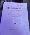
this is true innovation. give this man the Hero of Labor medal.A student thesis from the School of Marxism at China University of Petroleum, “Political Organization and Social Control of Humanity in Warhammer 40,000”.
View attachment 111566
- Status
- Not open for further replies.


