Chinese semiconductor thread II

tokenanalyst

Lieutenant General
Registered Member

Gezer Technology joins hands with the National Integrated Circuit Innovation Center to jointly build a 3-5nm advanced process joint engineering center​

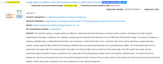
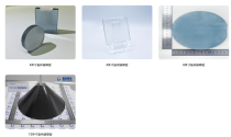
Gaize Technology and the National Integrated Circuit Innovation Center signed an agreement to establish an advanced integrated circuit process optical intelligent platform in Suzhou High-tech Zone. Positioned as a joint engineering center for 3-5 nanometer advanced processes, this project serves as an innovation platform for the domestic high-end integrated circuit manufacturing field, focusing on tackling key challenges in cutting-edge semiconductor testing technologies. After its implementation, the project will leverage a collaborative model between universities, enterprises, and research institutions to focus on overcoming core technological bottlenecks in advanced processes and third-generation semiconductor epitaxial testing.

Gaize Precision Technology (Suzhou) Co., Ltd. is a high-tech enterprise deeply involved in the semiconductor optical inspection field. Since settling in Suzhou High-tech Zone in 2021, it has continued to focus on the research and development of advanced process semiconductor metrology and inspection equipment and core optical components. It empowers optical inspection innovation with AI technology and has independently developed a complete set of semiconductor optical metrology and calibration solutions. It has formed an independent and controllable core technology system and patent matrix, and is a rising backbone enterprise in the field of domestic semiconductor optical intelligent inspection.
Please, Log in or Register to view URLs content!
 

tokenanalyst

Lieutenant General
Registered Member

The second national standard for gallium oxide, spearheaded by Fuga Gallium Industry, has passed the project approval public announcement.​


Hangzhou Fujia Gallium Industry Technology Co., Ltd. (Fuga Gallium) has achieved a significant milestone in the semiconductor sector with the official project approval and public announcement of its second national standard, titled "Test of Carrier Concentration in Gallium Oxide Epitaxial Layers by Capacitance-Voltage Method." This follows the company’s previous leadership in drafting the first national standard for "Gallium Oxide Single Crystal Polished Wafers." By spearheading these initiatives, Fuga Gallium is demonstrating a strong commitment to standardizing the ultra-wide bandgap semiconductor industry, aiming to resolve inconsistencies in testing methods that have historically hindered supply chain coordination and increased collaboration costs among substrate, epitaxial wafer, and device manufacturers.
1783696491032.png
The establishment of this new national standard addresses a critical bottleneck in the industrialization of gallium oxide (GaO), a core material for fourth-generation semiconductors known for its high breakdown electric field and suitability for high-power devices. Carrier concentration is a vital electrical parameter that directly influences the performance of power devices, yet testing methods have varied across institutions, leading to data incompatibility. The new standard provides an authoritative, unified technical basis for using the capacitance-voltage method to measure carrier concentration in GaO epitaxial layers. This uniformity serves as a "benchmark" for the industry, facilitating accurate quality evaluation, reducing communication costs, and laying the groundwork for large-scale mass production and international alignment.

Beyond this immediate achievement, Fuga Gallium is actively constructing a comprehensive standard system covering the entire "substrate-epitaxy" chain. The company is simultaneously advancing two additional national standards to further solidify the technical foundation of the GaO industry. As a National High-tech Enterprise and a leader in GaO material industrialization, Fuga Gallium continues to innovate in crystal growth equipment and wafer production. Their efforts not only enhance domestic technological self-reliance but also promote the high-quality development of the fourth-generation semiconductor sector by ensuring that technical specifications are rigorous, universally accepted, and conducive to rapid industrial scaling.
Please, Log in or Register to view URLs content!
 

tokenanalyst

Lieutenant General
Registered Member

The Beijing Academy of Quantum Sciences, in collaboration with Tsinghua University and Shanghai Jiao Tong University, has developed the first AI-enhanced low-temperature CMOS quantum measurement and control chip.​

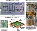
A collaborative team from the Beijing Academy of Quantum Information Science, Tsinghua University, and Shanghai Jiao Tong University has created the first quantum control chip that integrates artificial intelligence directly into its hardware. Published at the 2026 IEEE VLSI Symposium, this chip uses an on-chip neural network to automatically adjust qubit readings and correct for signal drift in real-time.

As quantum computers grow, connecting thousands of qubits to room-temperature electronics becomes impossible due to heat and space constraints. This chip moves critical processing inside the freezer (at 4 Kelvin), drastically reducing the number of wires needed.

Traditionally, AI calibration happens on powerful room-temperature computers. By embedding a lightweight neural network directly onto the cold chip, the system can react instantly to noise and instability without waiting for external commands, which is crucial for maintaining qubit coherence. The chip consumes only 10.3 mW total power. In ultra-low temperature environments, every milliwatt counts because cooling power is extremely limited and expensive. This efficiency makes scaling to larger processor sizes more feasible.

Specs:
  • Process: 28 nm CMOS (a mature, cost-effective semiconductor technology).​
  • Integration: Combines signal generation, reception, digital demodulation, and AI-based classification on a single chip.​
  • Performance: 1.9x lower transmitter power consumption compared to similar recent studies.​
This development marks a shift toward "quantum-intelligence fusion," where AI is not just used to analyze quantum data after the fact, but is embedded in the hardware to stabilize the quantum system itself. This is a critical step toward building practical, large-scale quantum computers that can operate reliably over long periods without constant manual recalibration.​

1783697262496.png

Please, Log in or Register to view URLs content!
 

tokenanalyst

Lieutenant General
Registered Member

The Institute of Microelectronics, Chinese Academy of Sciences, has made progress in the field of monolithic 3D heterogeneous​


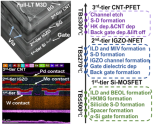
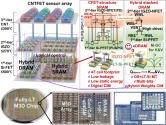
The team led by Yin Huaxiang from the Pilot Center of the Institute of Microelectronics, Chinese Academy of Sciences, in collaboration with the team led by Tang Jianshi from the School of Integrated Circuits, Tsinghua University, has proposed a fully low thermal budget "integrated sensing, storage, and computing" monolithic 3D prototype chip architecture for accelerating large-scale visual models.

In the post-Moore's Law era, the "geometric miniaturization" of traditional transistors has gradually slowed down, becoming a core bottleneck restricting the economic and large-scale development of high-performance AI chips. A new paradigm for integrated circuit development, represented by "τ's Law," has emerged, achieving a reduction in system-level latency and a significant increase in equivalent integration density through 3D stacking of multi-functional chips. At the edge, information processing also faces multiple challenges such as latency constraints, power consumption bottlenecks, and high data access overhead. Therefore, adopting a three-dimensional integrated architecture to vertically stack sensing units, cache units, and computing units on top of the core logic processing unit, constructing a low-latency, high-energy-efficiency edge AI chip integrating sensing, storage, and computing, has become an important direction for technological evolution.

Recently, a team led by Yin Huaxiang from the Pilot Center of the Institute of Microelectronics, Chinese Academy of Sciences, in collaboration with Tang Jianshi's team from the School of Integrated Circuits, Tsinghua University, proposed a low-thermal-budget, monolithic 3D integrated prototype chip architecture for accelerating large-scale visual models. This work vertically heterogeneously integrates multispectral carbon nanotube sensing units, 3D hybrid gain in-memory computing units, and hybrid CFET structure SRAM digital in-memory computing units within a single chip, and deeply aligns with the attention computation paradigm of DETR large-scale visual models. Compared to traditional 2D architectures, this effectively improves computational energy efficiency and processing time, providing a forward-looking technical path for edge AI visual computing.

1783697528652.png1783697542917.png

Please, Log in or Register to view URLs content!


Michael90

Senior Member
Registered Member
Please, Log in or Register to view URLs content!
This AI boom and memory price hike is crazy. There are companies making a fortune like never before . Samsung is now more peofitable than Nvidia itself which is crazy. In short, Samsung is now the most profitable country on earth due to memory/HBM.
Think about this : Samsung semiconductor is exected to make more profits this year than they have in their entire 40 years history in this industry, and their profit(not revenue) this year alone will be equivalent to Huawei's entire revenue last year. Yes you read that right . Its crazy, to think they have overtaken even Nvidia in profits margin.

Please, Log in or Register to view URLs content!

Please, Log in or Register to view URLs content!

So i shoulld exepect Chinese companies in this sector to easily grow their revenues and profits much more faster this year.
South Korea has really performed exceptionally well despite their tiny size. I'm actually amazed how competitive they have proven to be . Amazing accomplishments for such a small/medium country
 

tokenanalyst

Lieutenant General
Registered Member

Enhanced narrowband 6.7nm BEUV emission from laser-produced plasma based on foam-based Gd thin-film targets.​

Abstract​

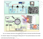
We experimentally investigated the 6.7 nm extreme ultraviolet (EUV) emission characteristics of laser-produced plasmas from foam-based Gd thin-film targets, demonstrating that a two-layer foam-supported target configuration yields a 20% enhancement in 6.7 nm EUV intensity. The effects of electrodeposition parameter optimization on the spectral characteristics of EUV emission were systematically investigated. The electrodeposition potential was tuned to control the elemental composition of the deposited layers, the deposition time to adjust the film thickness, and the electrolyte concentration was modulate the surface morphology. Compared to the bulk Gd target, the optimized foam-based target exhibited a 30% improvement in spectral purity and a 30% reduction in spectral bandwidth. This enhancement is attributed to porosity-induced alterations in both the structural integrity of the electrodeposited layer and laser energy coupling. Furthermore, Nomarski interferometry revealed that the foam-based Gd thin-film targets possess a lower and more spatially uniform electron density distribution than bulk Gd. These findings provide experimental validation for the feasibility of this target design as a promising candidate for future 6.7 nm EUV lithography sources.

1783701737997.png

Please, Log in or Register to view URLs content!
 

tphuang

General
Staff member
Super Moderator
VIP Professional
Registered Member
Please, Log in or Register to view URLs content!

an article on Nexchip's expansion plans as it looks to IPO in HKSE. In terms of capacity, it increased from 79.8k wpm to 139m wpm from 2023 to 2025. So far thru 4 months in 2026, it delivered 6.06m wafers.

Notice the R&D + focus for 22nm next generation platform.
 
Top