Chinese semiconductor thread II

tokenanalyst

Lieutenant General
Registered Member

Jingsheng Mechanical & Electrical accelerates the production of its 600,000-piece 8-inch SiC substrate project.​

Against the backdrop of the global energy revolution and semiconductor upgrade, silicon carbide (SiC) is accelerating its upgrade to larger sizes, and 8-inch SiC substrates are about to become the mainstream direction of the industry. The company's subsidiary, Zhejiang Jingrui Electronic Materials Co., Ltd., is fully accelerating the commissioning of its 600,000-piece annual production capacity 8-inch SiC substrate project and has started construction of a new phase of infrastructure. This expansion project will achieve unmanned automated operation and digital management, and will be built into an industry-leading fully automated intelligent factory.

In the field of integrated circuit equipment, the company has built a complete industrial chain layout for core equipment for 8-12 inch semiconductor silicon wafers, with product quality reaching international advanced levels and a leading domestic market share. Simultaneously, it has extended to chip manufacturing and packaging, with related products gaining market recognition and achieving mass sales. In the field of compound semiconductor equipment, the company's 6-8 inch silicon carbide epitaxial equipment, oxidation furnaces, and activation furnaces have achieved domestic substitution, with a leading market share in the industry. Since the beginning of this year, the company's semiconductor silicon wafer equipment, silicon carbide equipment, and chip manufacturing equipment businesses have progressed smoothly.

Please, Log in or Register to view URLs content!
 

huemens

Junior Member
Registered Member

China plans to let top AI firms buy limited Nvidia H200 chips, the Information reports​

Please, Log in or Register to view URLs content!
China is planning to allow the country's top AI companies to buy a limited number of Nvidia's H200 chips, the Information reported on Wednesday, citing two people with direct knowledge ‌of the matter.
Beijing is still determining the exact number of Nvidia chips to approve, and it could amount to fewer than 200,000 in total, the Information said, adding ⁠that was less than half of what the companies requested earlier this year.
Chinese officials have told Alibaba, ByteDance and DeepSeek in recent weeks that they may soon receive permission to buy some H200 chips, the report said.

Please, Log in or Register to view URLs content!
the government plans to let selected companies – including Alibaba Group Holding – buy limited numbers of the device, a source with knowledge of the matter told the South China Morning Post
 

huemens

Junior Member
Registered Member
Is this going to be China's equivalent of 2 more weeks from a nuclear weapon?
I also originally dismissed it when The Information posted it on Wednesday, because this news has been rehashed many times for months without any real outcome.
But posted it today because of the SCMP article where they corroborate it with their own sources. Since SCMP is owned by Alibaba they may have direct knowledge of it.
Notice in the SCMP article they mention Alibaba with their own sources but the other companies are referenced back to the original story from The Information.
government plans to let selected companies – including Alibaba Group Holding – buy limited numbers of the device, a source with knowledge of the matter told the South China Morning Post
Besides Alibaba, the Chinese government has also informed ByteDance – the maker of TikTok – and leading AI start-up DeepSeek of the coming approvals, though companies will have to explain why they need to buy the Nvidia product rather than a locally made alternative, The Information reported on Wednesday.
 

Hitomi

Junior Member
Registered Member
I also originally dismissed it when The Information posted it on Wednesday, because this news has been rehashed many times for months without any real outcome.
But posted it today because of the SCMP article where they corroborate it with their own sources. Since SCMP is owned by Alibaba they may have direct knowledge of it.
Notice in the SCMP article they mention Alibaba with their own sources but the other companies are referenced back to the original story from The Information.
Fair enough but I doubt the tech side of Alibaba will really talk to SCMP despite ownership. I will believe it when is see it. Reuters track record when it comes to tainting the information on AI is not new and is not going away recently, I will not take their word for it.
 

tokenanalyst

Lieutenant General
Registered Member

How to detect internal stress in wafers? Gezer ID300 offers a new domestic solution.​


Internal residual stress in silicon wafers is a common issue caused by temperature gradients, thermal expansion differences, lattice defects, and impurity distribution during the Czochralski growth process. This stress persists after dicing and can negatively impact yield and stability in subsequent manufacturing steps like grinding, polishing, and lithography.

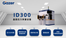
Gaze Intelligent Control Sensing Technology (Shanghai) Co., Ltd. (Gezer) has independently developed the ID300 wafer internal stress detection system. The ID300 wafer internal stress detection system is a new generation of wafer metrology equipment independently developed by Gezer based on its profound optical technology accumulation. The equipment integrates a self-developed high-precision optical system and intelligent measurement algorithms, which can perform rapid and non-destructive scanning and detection of internal residual stress on the entire wafer, and present the detection results in the form of an intuitive stress distribution map, realizing accurate analysis and visual characterization of the internal stress state of the wafer.


1783695160349.png


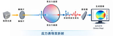
The ID300 utilizes high-precision optical technology based on the principle of birefringence. When stress distorts the wafer's lattice structure, it changes the refractive index in different directions. The system detects these subtle changes using self-developed optical systems and intelligent algorithms.
1783695141364.png

Gezer specializes in domestic semiconductor metrology equipment. Its product line includes FTIR and ellipsometry film thickness measurement, elemental analysis, and stress analysis. Their products have been verified by multiple wafer fabs and are in stable mass production. Gezer plans to leverage its AI optical intelligence platform to further integrate optical technologies with smart algorithms, aiming to enhance the self-sufficiency and quality of China’s semiconductor supply chain.​

Please, Log in or Register to view URLs content!
 

tokenanalyst

Lieutenant General
Registered Member

Gezer Optics achieves technological breakthrough: 100% self-developed and domestically produced core components such as laser light sources and spectrometers.​


Gezer Optics (Gaze Intelligent Control Sensing Technology) has successfully achieved 100% self-developed and domestically produced core components for high-end semiconductor metrology equipment, specifically laser-driven light sources and spectrometers.

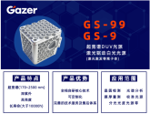
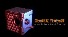
Gezer's self-developed GS-9 & GS-99 laser-driven light sources, based on proprietary optical technology, use laser-driven methods to excite xenon plasma at high energy. The output beam has a wide spectrum coverage of UV-VIS-NIR, and features high brightness and high stability. The lifespan of the light source is orders of magnitude higher than that of traditional light sources, providing a more stable and efficient light source solution for high-end optical measurement.

The GS-9 & GS-99 adopt a compact structural design and have advantages such as wide spectral coverage, small spot size and high stable output. They can be widely used in high-end optical scenarios such as spectral analysis, film thickness measurement, wafer inspection, calibration optical systems and spectrophotometric detection.

1783695462292.png1783695364555.png


Leveraging its AI optical intelligence platform, Gezer has established a complete optical technology system covering core devices, optical systems, and algorithm platforms. The products have passed verification by multiple wafer foundries and FAB customers and have entered stable mass production, marking a significant step in the localization and self-reliance of China’s high-end semiconductor metrology supply chain. Gezer plans to continue R&D investment to further drive the localization of core technologies and provide competitive domestic solutions for advanced semiconductor manufacturing processes.

Please, Log in or Register to view URLs content!
 
Top