You are using an out of date browser. It may not display this or other websites correctly.
You should upgrade or use an alternative browser.
You should upgrade or use an alternative browser.
Chinese semiconductor thread II
- Thread starter vincent
- Start date
Rockchip launches RK182X series AI coprocessors.
On November 26, Rockchip launched the RK182X series, a high-performance AI coprocessor designed for edge-side AI inference. Featuring a multi-core NPU, it supports local deployment of large language models (LLMs) and vision-language models (VLMs) with up to 7B parameters, enabling efficient processing of text and image data.
Include:
Include:
- Built-in 2.5GB or 5GB DRAM integrated via 3D stacking, achieving high bandwidth (theoretically up to 1TB/s) and compact design.
- Connects to host systems via PCIe 2.0 or USB 3.0, allowing seamless addition of AI computing power to existing PCs, industrial devices, and embedded systems offering a "lightweight upgrade" path.
- Capable of generating over 100 tokens per second, improving inference speed in local model usage.
This move aligns with the growing demand for edge AI and privacy-sensitive applications, enabling faster response times, better data security, and offline functionality in personal computers, AI terminals, and industrial devices.
Changguang Huaxin: 100G EML chip has entered mass production, and 200G EML is in the sampling stage.
Changguang Huaxin disclosed in an announcement that, driven by the continued growth in computing power demand, the company's high-end optical chip product line is progressing steadily. Among them, the 100G EML chip has achieved mass production and shipment, and the 200G EML chip has entered the customer sampling stage. The relevant products are mainly aimed at high-speed optical communication and data center scenarios.
The company stated that as applications such as AI and big data drive a rapid increase in data center bandwidth demand, the importance of high-performance optical chips in cloud computing and backbone network transmission is becoming increasingly prominent. Devices such as EML (externally modulated laser), VCSEL, and DFB are key components for achieving high-speed and stable optical interconnects, and have a direct impact on the performance and energy efficiency of optical modules.
The announcement indicates that, in addition to the 100G EML achieving mass production and the 200G EML entering the sampling stage, the company's 100G VCSEL, 100mW continuous wave (CW) DFB, and 70mW CWDM4 DFB chips have all reached mass production and shipment levels. These products were previously disclosed in the company's semi-annual report; this reiteration aims to update the market on the relevant technological and industrialization progress.

Changguang Huaxin also cautioned that although the aforementioned high-end optical chip products have entered the mass production or sampling stage, their actual contribution to this year's sales and profits remains uncertain. The company emphasized that product development progress, customer sample testing results, product introduction pace, and market expansion are all subject to multiple factors, including industry competition, downstream investment pace, and changes in technological routes, resulting in certain uncertainties and risks in the related business.
The company stated that as applications such as AI and big data drive a rapid increase in data center bandwidth demand, the importance of high-performance optical chips in cloud computing and backbone network transmission is becoming increasingly prominent. Devices such as EML (externally modulated laser), VCSEL, and DFB are key components for achieving high-speed and stable optical interconnects, and have a direct impact on the performance and energy efficiency of optical modules.
The announcement indicates that, in addition to the 100G EML achieving mass production and the 200G EML entering the sampling stage, the company's 100G VCSEL, 100mW continuous wave (CW) DFB, and 70mW CWDM4 DFB chips have all reached mass production and shipment levels. These products were previously disclosed in the company's semi-annual report; this reiteration aims to update the market on the relevant technological and industrialization progress.

Changguang Huaxin also cautioned that although the aforementioned high-end optical chip products have entered the mass production or sampling stage, their actual contribution to this year's sales and profits remains uncertain. The company emphasized that product development progress, customer sample testing results, product introduction pace, and market expansion are all subject to multiple factors, including industry competition, downstream investment pace, and changes in technological routes, resulting in certain uncertainties and risks in the related business.
Hesai has released its self-developed RISC-V LiDAR main control chip, the Fermi C500, featuring a 256-line ATX upgrade.
On November 24th, Hesai Technology a global leader in LiDAR, held its 2025 Technology Open Day at the Hesai Maxwell Global R&D and Manufacturing Center in Shanghai. Dr. Sun Kai, co-founder and chief scientist of Hesai Technology, delivered a keynote speech on the theme "LiDAR: Raising the Upper Limit or Maintaining the Lower Limit," and unveiled the Fermi C500 , a high-performance intelligent main control chip for LiDAR based on the RISC-V architecture. Hesai also launched the world's only "photonic isolation" security technology and a refreshed version of its 256-line secure LiDAR ATX. Currently, the "photonic isolation technology" has been fully implemented in Hesai's ATX and ETX main LiDAR systems, offering industry-leading security and reliability, achieving a physical-level "zero false alarm" capability.
With a cumulative delivery of 185 million units, the final piece of the puzzle has been completed through self-developed full-stack technology.
The Fermi C500 , a high-performance intelligent main control chip for Hesai's LiDAR , completes the puzzle of Hesai's fourth-generation chip platform, which is entirely self-developed. The Fermi C500 adopts an independently controllable RISC-V architecture, ensuring supply chain security and independent technological iteration. This single-chip integrates an MCU, FPGA, and ADC, making it the world's first LiDAR-specific main control chip with dual certifications for functional safety and network security, meeting the stringent reliability and information security requirements of automotive scenarios at the hardware level. It is also the world's first LiDAR-specific main control chip with a built-in point cloud intelligent engine (IPE) , integrating a 256-core waveform processing core for intelligent environmental noise filtering, adapting to complex weather conditions, and providing all-weather high-precision perception for autonomous driving.
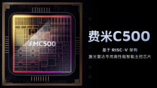
Hesai began developing dedicated ASIC chips for LiDAR in 2017. By simplifying product architecture and optimizing design, it has significantly improved performance, quality, and cost-effectiveness, giving the company a significant advantage in the fierce market competition. Its chip products have achieved full-scale mass production, forming a solid technological barrier. Several years ago, Hesai predicted that chip-based transceiver architecture would be the only ultimate solution for LiDAR; therefore, a top-tier LiDAR company must also be a top-tier chip company.
After four generations of chip platform development, Hesai is currently the only LiDAR company in the industry that has achieved full-stack self-development of seven key components, including lasers, detectors, laser drivers, TIA chips, ADC chips, digital signal processors, and controllers (1) . As of November 2025, Hesai has 16 self-developed chips that have obtained AEC-Q automotive-grade certification, and has delivered a total of 185 million chips (2) , ranking first in the world. With its self-developed chip path, Hesai Technology has developed a strong product line, including the AT, ET, and FT series, as well as the XT, OT, and JT series. These products have quickly gained market recognition and won many mass production orders at home and abroad.
AMEC patent for a plasma processing device and a method for preventing plasma leakage, aiming to avoid plasma leakage.
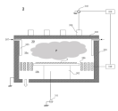
According to information from the State Intellectual Property Office, Advanced Micro-Fabrication Equipment (Shanghai) Co., Ltd. has applied for a patent entitled "A Plasma Processing Device and a Method for Preventing Plasma Leakage", with publication number CN 121011490 A and application date of May 2024.
The patent abstract shows that the present invention provides a plasma processing apparatus and a method for preventing plasma leakage. The apparatus includes: a reaction chamber with a base for supporting a wafer, the base being electrically connected to a first non-constant voltage power supply; a constraint ring surrounding the outer periphery of the base, dividing the space within the reaction chamber into a plasma processing area and an exhaust area connected to an external vacuum pump; the constraint ring being electrically connected to a second non-constant voltage power supply; and the constraint ring preventing plasma from entering the exhaust area. Even when the plasma density within the reaction chamber is high, the present invention can prevent plasma leakage and ensure that the airflow conduction of the constraint ring meets process requirements.
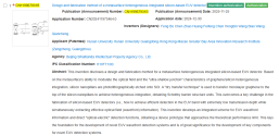
Tsinghua University and Huahai Qingke have receive patents for a wafer support devices and a wafer cleaning devices to ensure reliable wafer support.
According to information from the State Intellectual Property Office, Tsinghua University and Huahai Qingke Co., Ltd. have applied for a patent entitled "A Wafer Support Device and a Wafer Cleaning Device", with publication number CN120998864A and application date of December 2019.
The patent abstract reveals that this invention discloses a wafer support device and a wafer cleaning device. The wafer support device includes a support assembly that moves to horizontally support the wafer; at least one support assembly can swing relative to its direction of movement to adjust its position. The wafer support device of this invention ensures that the support rollers make uniform contact with the outer edge of the wafer, guaranteeing reliable wafer support. A cleaning brush located on the side of the wafer effectively removes impurities from the wafer surface, achieving wafer surface cleaning.
China Electronics Technology Group Corporation (CETC) has successfully developed a high-output-power diamond photoconductive switching device.
Recently, the research team of the Key Laboratory of the Industrial Basic Research Institute of China Electronics Technology Group Corporation (CETC) made a breakthrough in key core technologies and successfully developed a diamond photoconductive switch device with high output power, which strongly promotes the practical application of diamond in the field of photoconductive switches.
Photoconductive switches, as core devices in high-power and ultrafast electronics, utilize laser pulses for triggering and can be widely used in scenarios requiring high speed, high power, and strong anti-interference capabilities, such as smart grid switches and pulsed power systems. Diamond, with its superior material properties, has become an ideal candidate material for realizing high-performance photoconductive switches. The research team at the Key Laboratory of the Industrial Foundation Research Institute addressed the challenges of high on-resistance and susceptibility to surface flashover in diamond photoconductive switches by optimizing the doping concentration design and employing surface passivation technology. They successfully developed a high-output-power diamond photoconductive switch device, effectively reducing the device's on-resistance, significantly suppressing surface flashover, and substantially improving the device's withstand voltage.
Photoconductive switches, as core devices in high-power and ultrafast electronics, utilize laser pulses for triggering and can be widely used in scenarios requiring high speed, high power, and strong anti-interference capabilities, such as smart grid switches and pulsed power systems. Diamond, with its superior material properties, has become an ideal candidate material for realizing high-performance photoconductive switches. The research team at the Key Laboratory of the Industrial Foundation Research Institute addressed the challenges of high on-resistance and susceptibility to surface flashover in diamond photoconductive switches by optimizing the doping concentration design and employing surface passivation technology. They successfully developed a high-output-power diamond photoconductive switch device, effectively reducing the device's on-resistance, significantly suppressing surface flashover, and substantially improving the device's withstand voltage.

