Chinese semiconductor thread II

tokenanalyst

Lieutenant General
Registered Member

Actively embracing RISC-V+AI, NationalChip Technology's high-performance automotive intelligent domain control AI MCU chip has completed design and entered the tape-out trial production stage.​


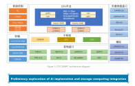
NationalChip Technology has launched the CCFC3009PT, a landmark high-end automotive AI MCU chip based on RISC-V architecture with a 6+6-core design (6 main + 6 lockstep cores, configurable for user needs). The chip delivers over 10,000 DMIPS computing power and integrates a dedicated NPU (Neural Processing Unit), making it ideal for intelligent automotive domain control applications.
1760021198969.png

Main Features:​
  • Use of 22nm RRAM memory technology, offering triple improvements in storage density, read/write speed, and power efficiency over traditional solutions.​
  • Deep integration of AI capabilities via "hardware acceleration + toolchain adaptation," enabling developers to use proven edge AI methods with reduced entry barriers.​
  • A novel RRAM-NPU co-design approach that combines high-performance NPU logic with in-memory computing using RRAM arrays. This reduces data movement energy and enables more efficient matrix operations (e.g., matrix-vector multiplication) for neural networks—laying the foundation for future integrated storage-computing AI platforms.​

Core Application Scenarios:​

  1. Radar Signal Processing: Enhances object classification, free-space segmentation, and micro-Doppler analysis to improve perception accuracy ("seeing and understanding" objects).​
  2. Battery Management System (BMS): Enables accurate health estimation, cell balancing optimization, and thermal runaway prediction.​
  3. Motor Control: Supports real-time parameter self-tuning and fault prediction for improved efficiency and safety in electric steering/brakes.​
  4. Sensor Fusion & Decision-Making: Acts as an intelligent gateway in domain controllers, fusing radar/camera data and enabling local decisions (e.g., detecting driver fatigue).​

Forward-Looking Features:​

  • Native support for virtualization to enable efficient multitasking and dynamic resource management.​
  • Onboard network routing module that handles CAN-to-Ethernet packet forwarding, freeing up CPU resources.​
  • Advanced security with HSM subsystem, including quantum-resistant cryptography compliant with FIPS 203/204 standards.​

Strategic Significance:​

The CCFC3009PT embodies the trend of "edge AI" and intelligent sensing in smart vehicles—bringing AI intelligence to sensors and subsystems for faster, more reliable, real-time processing. It reduces central compute load, improves system efficiency, and is a key component in building "software-defined cars."

This achievement marks a major step forward in China’s domestic automotive MCU development—pushing the industry toward high-performance, intelligent, secure, and energy-efficient solutions. NationalChip plans to expand its chip ecosystem through hardware-software collaboration, aiming to deliver competitive, next-generation AI-enabled automotive electronics for future smart vehicles.

Please, Log in or Register to view URLs content!
 

tonyget

Senior Member
Registered Member
TechInsights are included in the unreliable entity list by Chinese Ministry of Commerce

Please, Log in or Register to view URLs content!


1. 反无人机技术公司(Dedrone by Axon)

2. 迪杰恩技术公司(DZYNE Technologies)

3. 埃比特系统美国分公司(Elbit Systems of America, LLC)

4. 伊比鲁斯公司(Epirus, Inc.)

5. 宇航环境公司(AeroVironment, Inc.)

6. Exelis公司(Exelis Inc.)

7. 联合技术系统运营公司(Alliant Techsystems Operations LLC)

8. 贝宜系统股份有限公司(BAE Systems, Inc.)

9. Teledyne FLIR公司(Teledyne FLIR, LLC)

10. VSE公司(VSE Corporation)

11. 立方全球防务公司(Cubic Global Defense)

12. Recorded Future公司(Recorded Future, Inc.)

13. 哈利法克斯国际安全论坛 (Halifax International Security Forum)

14. TechInsights公司(TechInsights Inc.)及其分支机构

-TechInsights Inc.

-TechInsights Europe Limited

-TechInsights Europe Sp zo.o

-TechInsights Japan KK

-TechInsights USA Inc

-TechInsights Korea Co. Ltd.

-TechInsights Market Analysis Limited

-SARL Strategy Analytics

-Strategy Analytics GmbH Market Research and Management Consulting

-SARI Strategy Analytics Private Limited
 

tokenanalyst

Lieutenant General
Registered Member
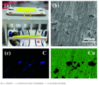
At the 2025 International Conference on Electronic Packaging Technology (ICEPT 2025) , a team from Huazhong University of Science and Technology presented their latest research findings, "Near-junction heat dissipation of high-power chips by copper-diamond-based heat sink." The team proposed a copper-diamond heat sink (CDHS) based on an electrodeposition process , achieving near-junction heat dissipation for high-power chips .

The main innovations include:​
  • The copper-diamond composite layer is deposited directly on the back of the aluminum substrate by electroplating , which has a mild process, simple equipment and low energy consumption;​
  • By adjusting the plating solution parameters and stirring rate, diamond particles (40 μm) are evenly distributed in the copper matrix, forming a continuous heat conduction network.​
  • The chip (LED) is directly soldered to the composite layer to achieve an integrated chip-heat sink structure and reduce interface thermal resistance.​

1760042659371.png

This work demonstrates the potential of electrodeposition composite technology for high-thermal-conductivity metal-matrix composites . Compared to currently common, high-cost routes like powder metallurgy and hot pressing, electrodeposition can be directly integrated onto the backside of the package substrate, promising an intermediate technology that balances performance and manufacturing efficiency . This is particularly applicable to applications with high near-junction heat flux densities, such as LED lighting, power modules, and RF devices.

In high heat flux density applications such as power electronics, radio frequency modules, and third-generation semiconductor device packaging, copper-diamond composites are expected to:​
  • Replace some copper-molybdenum and copper-tungsten substrates to achieve higher thermal conductivity;​
  • Complementary to aluminum nitride and silicon nitride ceramic substrates ;
  • Promote the evolution of chip-level thermal management towards near-junction area and integration.​
Achieving efficient heat dissipation through low-cost processes is expected to push diamond composite materials from the laboratory to engineering applications.

Please, Log in or Register to view URLs content!
 

tokenanalyst

Lieutenant General
Registered Member

Fudan University releases the world's first two-dimensional-silicon hybrid architecture chip.​


a research team from Fudan University published their latest findings in the international journal Nature . Titled " A full-featured 2D flash chip enabled by system integration," they demonstrated the world's first 2D-silicon hybrid architecture flash memory chip. This breakthrough marks a milestone for Chinese research teams in the engineering and systemic application of 2D electronic devices.

The research was led by a team from the National Key Laboratory of Integrated Chips and Systems and the School of Integrated Circuits and Micro-Nanoelectronics at Fudan University. In April of this year, the team published a prototype of their "PoX" 2D picosecond flash memory device in Nature, achieving ultra-fast non-volatile memory at 400 picoseconds, setting a new semiconductor memory speed record. This time, they further integrated the PoX device with mature silicon-based CMOS processes to develop a 2D-silicon hybrid architecture, codenamed "Changying (CY-01)," achieving the leap from atomic-scale devices to functional chips.
1760042822007.png
Beautiful picture.

The team believes that memory is the most promising area for industrialization of two-dimensional electronic devices. By integrating traditional CMOS processes, they have successfully achieved the coordinated integration of two-dimensional memory modules with silicon-based circuits. This enables the chip to support 8-bit instruction operations, 32-bit parallel operation, and random addressing, with a yield rate of 94.3%. This performance surpasses existing Flash technology in all respects, demonstrating strong system-level feasibility.

Innovative integration process: Achieving atomic-level fusion of two-dimensional materials and CMOS​


Two-dimensional materials differ significantly from traditional silicon-based materials in thickness, structure, and process compatibility. After five years of research, the team developed a modular integration solution: The two-dimensional memory module and CMOS control circuitry are fabricated separately, then precisely coupled via high-density monolithic interconnects (micrometer-scale vias). This approach effectively avoids the risk of production line contamination and ensures stable bonding of the two-dimensional material to the complex CMOS substrate.

The team also proposed a "2D-CMOS cross-platform system design methodology," encompassing collaborative design, interface design, and system-level verification. They named the overall integrated framework the "Changying (CY-01) Architecture." This core process breakthrough represents a crucial step forward in the engineering of 2D materials, laying the foundation for their industrial application.

Achieving Million-Scale Integration in 3-5 Years: The "China Path" from Lab to Factory​

Relying on the completed tape-out results, the team plans to promote the large-scale integration of chips to the million-level in the next 3-5 years, and build an independent and leading engineering project platform to form a licensable intellectual property system.

In the era of artificial intelligence and big data, the bottleneck in computing power development is gradually shifting from front-end computing to back-end storage. Industry experts believe that the speed and energy efficiency advantages of a 2D-silicon hybrid architecture are expected to revolutionize traditional flash memory systems and provide more efficient storage solutions for AI, mobile devices, servers, and other scenarios.

"This achievement is not a continuous improvement, but a disruptive advancement in speed and efficiency." Industry insiders said that its "science-engineering-system" closed-loop model has opened up an original Chinese path for the new generation of storage technology.
The team said that in the future, the "Changying (CY-01)" architecture is expected to become the standard storage solution for the AI era, providing higher speed and lower energy consumption support for cutting-edge fields such as artificial intelligence and big data, allowing two-dimensional flash memory to lead information technology into a new high-speed era.​

Please, Log in or Register to view URLs content!
 

tphuang

General
Staff member
Super Moderator
VIP Professional
Registered Member

pretty good one on how Rare earth is used in semiconductor

先进半导体工艺和设备对于稀土材料的依赖 半导体产业作为现代科技的核心支柱,其发展在很大程度上依赖于稀土元素所具备的独特化学与物理特性。这些元素,包括镧(La)系元素,钇(Y)和钪(Sc),在导电性,介电性能以及气体敏感特性方面发挥着关键作用,对提升半导体器件的性能至关重要。 例如,钕(Nd)是制造半导体设备中高性能永磁体(如步进电机,高精度定位系统)的关键材料,而镝(Dy)的加入则可显著提升磁体在高温环境下的稳定性与抗退磁能力。铕(Eu)则在显示技术中不可或缺,是荧光粉的重要组成部分,广泛用于液晶与OLED显示器。
lanthanides (La), yttrium (Y), and scandium (Sc), play a key role in electrical conductivity, dielectric properties, and gas sensitivity, and are crucial to improving the performance of semiconductor devices. Scandium and yttrium are in the covered list

在半导体工艺领域,稀土氧化物也不可替代。氧化铈(CeO₂)是化学机械平坦化(CMP)工艺的核心材料,其抛光浆料直接影响晶圆的平整度与最终良率。对于高层数NAND闪存而言,CMP质量的稳定性尤为关键,任何抛光颗粒短缺或质量波动都会放大次品率。 近年来,氧化镧(La₂O₃),氧化钆(Gd₂O₃)与氧化镥(Lu₂O₃)等高介电常数(High-k)稀土氧化物因其优异的热稳定性与介电特性,被广泛研究用于逻辑和存储芯片。另外,随着原子层沉积(ALD)技术的进步,特别是采用臭氧(O₃)等替代氧化剂的工艺创新,稀土氧化物薄膜的均匀性与稳定性显著提升,使其在先进制程中更具可行性。 此外,一氧化钇(YO)等二价稀土氧化物也被合成为外延薄膜,展现出独特的电子与磁性特征。其可调控的电导率,窄带隙以及强自旋轨道耦合特性,使其成为新一代半导体器件材料的重要候选。 在特定半导体材料体系中,稀土掺杂技术同样不可或缺。例如,在高速,高频器件使用的氮化镓(GaN)与磷化铟(InP)材料中,钇(Y)和铕(Eu)常被用于提升载流子迁移率与光电转换效率,我们之前聊过市场非常关注的光模块需要;而稀土掺杂的氧化铟(In₂O₃)表现出显著增强的气体传感性能,拓展了其在智能感知芯片中的应用前景。
Cerium oxide in CMP (but cerium is not included) Same with lanthanum oxide
Gadolinium oxide (Gd₂O₃), and lutetium oxide (Lu₂O₃) are used in High-K MG, so that's going to be problematic (and they are in the list)
yttrium monoxides in epitaxial thin film, so that's a problem one
Also yttrium is used in RF materials like GaN and InP. I don't see how China could allow these to be permitted.
not sure why Indium keeps getting mentioned here

在半导体设备领域,稀土材料也贯穿多个关键环节。以EUV光刻机为例,其核心技术主要包括三项:顶级的光源系统,高精度的物镜系统以及工件台。这些均需要使用稀土材料,比如说使用NdFeB永磁体(步进电机以及高精度定位系统)与掺杂了稀土元素晶体的固体激光器;而刻蚀与沉积设备的真空腔体,靶材表面常采用Y₂O₃、CeO₂等稀土氧化物涂层,以提升耐蚀性与使用寿命。
again, looks like Cerium, yttrium and permanent magnet in SMEs, especially like EUV.

至于后段封装与测试环节,高端封装中使用的导热陶瓷,荧光掺杂封装材料,以及用于光电探测器的稀土掺杂晶体,虽然用量不大,却在特定高性能应用(如高频雷达、红外传感和量子器件)中具有不可替代的作用。 所以,稀土元素贯穿半导体制造的几乎每个环节,从材料到设备,从工艺到封装测试,其重要性远超传统金属原料。一旦稀土供应链受到出口管制,价格波动或精炼环节受限,全球先进芯片生产链都将不可避免地面临结构性影响。
in back end packaging, all the high end radar, IR and quantum devices all use Rare earth.

so it's pretty widely used and not something you can just replace quickly.
 

tokenanalyst

Lieutenant General
Registered Member

pretty good one on how Rare earth is used in semiconductor


lanthanides (La), yttrium (Y), and scandium (Sc), play a key role in electrical conductivity, dielectric properties, and gas sensitivity, and are crucial to improving the performance of semiconductor devices. Scandium and yttrium are in the covered list


Cerium oxide in CMP (but cerium is not included) Same with lanthanum oxide
Gadolinium oxide (Gd₂O₃), and lutetium oxide (Lu₂O₃) are used in High-K MG, so that's going to be problematic (and they are in the list)
yttrium monoxides in epitaxial thin film, so that's a problem one
Also yttrium is used in RF materials like GaN and InP. I don't see how China could allow these to be permitted.
not sure why Indium keeps getting mentioned here


again, looks like Cerium, yttrium and permanent magnet in SMEs, especially like EUV.


in back end packaging, all the high end radar, IR and quantum devices all use Rare earth.

so it's pretty widely used and not something you can just replace quickly.
This will increase the cost of semiconductor manufacturing for those affected. Is not just one item, is a lot criticals materials in that list.
 
Top