Chinese semiconductor thread II

tphuang

General
Staff member
Super Moderator
VIP Professional
Registered Member

this is rather interesting. Again, we will see how this affects things.

三、针对先进芯片与AI用途的“逐案审批” 值得注意的是,公告特别指出: 凡最终用途涉及研发或生产14纳米及以下逻辑芯片,256层及以上存储芯片,或相关的半导体设备,测试设备和材料,以及用于研发具有潜在军事用途的人工智能技术的出口申请,将实行逐案审批制度。

I'm pretty sure nvidia chips use heavy rare earth metals.
 
Last edited:

tphuang

General
Staff member
Super Moderator
VIP Professional
Registered Member
Does the R&D include patents/licensing? Like ymtc to samsung thing?

for no.1, 2nd bullet, can be applied to the alleged joined venture in Malaysia..
let's keep non semi related commentary for science & tech thread where I will also post this.
 

tphuang

General
Staff member
Super Moderator
VIP Professional
Registered Member
Please, Log in or Register to view URLs content!

Fudan university researchers published paper on Nature about "full-featured 2D flash chip enabled by system integration)

基于 CMOS 电路控制二维存储核心的全片测试支持 8-bit 指令操作,32-bit 高速并行操作与随机寻址,良率高达 94.3%。这也是迄今为止世界上首个二维-硅基混合架构闪存芯片,性能“碾压”目前的 Flash 闪存技术,首次实现了混合架构的工程化。

“从第一个原型晶体管到第一款 CPU 花了大约 24 年,而我们通过把先进技术融入工业界现有的 CMOS 产线,这一原本需要数十年的积累过程被大幅压缩,未来可以进一步加速探索颠覆性应用。”刘春森总结。
Full-chip testing of the CMOS-based circuit-controlled two-dimensional memory core supports 8-bit instruction operations, 32-bit high-speed parallel operations, and random addressing, achieving a yield rate of 94.3%. This is also the world's first 2D-silicon hybrid architecture flash memory chip, surpassing existing Flash technology in performance and achieving the first engineering feasibility of a hybrid architecture.
 

tokenanalyst

Lieutenant General
Registered Member

Sifang Optoelectronics plans to invest 600 million yuan to build a high-end sensor industry base​

Sifang Optoelectronics issued an announcement that it plans to invest in the construction of a high-end sensor industry base in the Optics Valley Optoelectronics Information Industry Park in the Wuhan East Lake New Technology Development Zone. The total investment amount of the project is 600 million yuan.
According to the announcement, this investment will include 400 million yuan in fixed assets and 200 million yuan in R&D. Sifang Optoelectronics has signed an investment cooperation agreement with the Wuhan Optics Valley Optoelectronics Information Industry Park Construction Service Center. This project will provide strong resource support for the company's future development.
Sifang Optoelectronics stated that the project will leverage the policy advantages and locational advantages of the Wuhan East Lake New Technology Development Zone to build a new headquarters campus, encompassing a research and development center, a marketing center, and a management center. Furthermore, the project will include a manufacturing base, focusing on developing production capabilities for key equipment such as actuators and controllers.
Through this investment, Sifang Optoelectronics plans to integrate its existing R&D resources and industrialization capabilities to further enhance its R&D capabilities and production scale. This will effectively bolster the company's market competitiveness in the high-end sensor sector and help achieve its long-term development strategy.
Industry analysts pointed out that with the continued growth in demand for high-end sensors, Sifang Optoelectronics will occupy an important position in the industrial chain through this layout, further strengthening its industry influence in the optoelectronics and sensor fields.

Please, Log in or Register to view URLs content!
 

tokenanalyst

Lieutenant General
Registered Member

Nantong Jianzhen high-end equipment parts manufacturing project with a total investment of 3 billion yuan started​

On October 8, construction began on the Nantong Jianzhen High-End Equipment Parts Manufacturing Project in the Haimen Economic and Technological Development Zone. The project is reportedly funded with a total investment of 3 billion yuan, including 1.5 billion yuan in the first phase, covering 200 mu (approximately 16 acres) of land and 800 million yuan in production equipment. The project aims to overcome bottlenecks in core equipment production and establish an ultra-precision manufacturing base.

1760019564526.png

The project investor, Changchun Jianzhen Precision Machinery Manufacturing Co., Ltd., established in 2016, is a national-level "Little Giant" enterprise specializing in specialized, high-tech, and innovative industries. It is also a designated "Gazelle Enterprise" in Jilin Province. Leveraging resources from renowned domestic research institutes and universities, the company undertakes high-precision component processing and assembly projects. Its main products include high-precision parts made of both metal and non-metallic materials, including the processing of specialty materials like Invar and titanium alloys, as well as precision shafting, guide rails, and other components, as well as complete machine assembly. These products are widely used in industries such as aerospace, satellites, optoelectronic theodolites, integrated circuits, and semiconductor equipment.

Please, Log in or Register to view URLs content!
 

tokenanalyst

Lieutenant General
Registered Member

VeriSilicon expects record Q3 revenue and orders exceeding 1.5 billion​


VeriSilicon Microelectronics (Shanghai) Co., Ltd. issued an announcement on October 8, predicting that its operating income in the third quarter of 2025 will reach 1.284 billion yuan, a record high for the company, a month-on-month increase of 119.74% and a year-on-year increase of 78.77%.
The company also expects profitability to improve significantly in the third quarter, with losses narrowing significantly both year-on-year and quarter-on-quarter, but still not turning a profit. In the first half of 2025, VeriSilicon's operating income was 974 million yuan, a year-on-year increase of 4.49%.
VeriSilicon stated that the significant performance increase was primarily due to the strong performance of its one-stop chip customization services. Specifically, the company expects third-quarter chip design revenue to be 429 million yuan, a 291.76% increase from the previous quarter and an 80.67% year-on-year increase. Its mass production revenue is expected to be 609 million yuan, a 133.02% increase from the previous quarter and a 158.12% increase from the previous year. Its intellectual property licensing fees are expected to be 213 million yuan, a 14.14% increase from the previous quarter.
VeriSilicon also achieved record growth in orders. New orders for the third quarter are expected to reach 1.593 billion yuan, a significant year-on-year increase of 145.80%. By the first three quarters of 2025, new orders totaled 3.249 billion yuan, exceeding the full-year new order level for 2024. AI computing power-related orders accounted for approximately 65% of this total.

Please, Log in or Register to view URLs content!
 

tokenanalyst

Lieutenant General
Registered Member

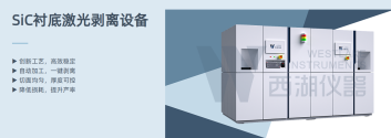
West Lake Instruments Product Demonstration Center was completed and put into trial operation​

Recently, the product demonstration center of West Lake Instrument (Hangzhou) Technology Co., Ltd. (referred to as "West Lake Instrument") was completed and put into trial operation.

The center is a comprehensive platform that integrates an 8-inch silicon carbide laser lift-off automated production line and large-size silicon carbide substrate processing verification. It has the verification capability of cutting-edge technologies and products. It is a key carrier for promoting laser lift-off technology from "process feasibility" to "mass production and ease of use", and can provide customers with all-round support from process introduction to mass production decision-making.

1760019993818.png

As the core of the product demonstration center, the 8-inch SiC laser lift-off automated production line achieves full automation and unmanned operation from ingot to wafer, making it a powerful industrial tool for meeting current market demands and achieving cost reduction and efficiency improvement. The verification line produces over 20,000 8-inch substrates annually. Its modular design allows for flexible capacity allocation and provides customers with comprehensive, multi-level verification data.

The large-scale SiC laser lift-off process verification line primarily serves new technology and product validation for 12-inch SiC substrates. With an annual production capacity of over 10,000 12-inch substrates, it can also meet the processing needs of various non-standard large-scale seed crystals. Its core mission is to overcome large-scale process challenges, conduct forward-looking technological research and development, and provide technical reserves and solutions for the next generation of large-scale substrate processing.

Please, Log in or Register to view URLs content!
 

tokenanalyst

Lieutenant General
Registered Member

Towards finer 4H-SiC slicing: a spatiotemporally tailored combined pulse​

Abstract​


Laser slicing of 4H-SiC can achieve low kerf loss and high efficiency, but it produces a rough surface degrading, processing quality. This Letter proposes a spatiotemporally tailored combined pulse (STT-CP) method, utilizing wavefront and temporal shaping of picosecond (ps) and nanosecond (ns) lasers based on the polarization state-dependent properties of the spatial light modulators, enabling aberration-free single ps laser focus with dual ns foci at different focal positions inside the material. This way, modification enhancement with a spatiotemporal interval is demonstrated, achieving 9 times larger internal modification width inside 4H-SiC than single ps pulse modification. Furthermore, a finer 4H-SiC wafer with a surface roughness of 93 nm and a slicing groove depth of 440 nm is sliced with dual ns laser foci separated by 5 μm at 100 ns time delay after the ps laser, highlighting the potential for finer material processing.

Please, Log in or Register to view URLs content!
 

tokenanalyst

Lieutenant General
Registered Member

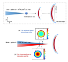
Enhanced extreme ultraviolet emission from a transverse profile-tailored laser-driven preformed tin disk targets.​

Abstract​

Highly efficient in-band extreme ultraviolet (EUV) generation from a confined plasma, produced by a 1-μm wavelength transverse-profile-tailored laser-irradiated preformed disk target, has been demonstrated via radiation hydrodynamic simulations. The tailored laser exhibits a crater-like intensity profile, with a lower intensity at the center and a higher intensity in the surrounding annular region. It is found that such an intensity profile can confine plasmas by driving inward plasma flow, which induces ion density accumulation. The confined plasma can effectively convert part of the expanding plasma kinetic energy into thermal energy for further radiative energy conversion. Further investigations into the in-band radiation emissivity and optical depth show that although the self-absorption effect in the confined plasma is relatively significant, the increase in emitter density ultimately boosts the final conversion efficiency (CE). Eventually, the light source generated by the tailored laser achieves a CE of 4.1%, which is 20% higher than that of the Gaussian laser (3.5%) under the same conditions. This study highlights a promising pathway for advancing efficient EUV source generation by modulating the laser transverse profile.

1760020353217.png

Please, Log in or Register to view URLs content!
 
Top