
You are using an out of date browser. It may not display this or other websites correctly.
You should upgrade or use an alternative browser.
You should upgrade or use an alternative browser.
Chinese semiconductor thread II
- Thread starter vincent
- Start date


Ministry of Industry and Information Technology: Profits of equipment manufacturing industry increased by 7.2% year-on-year from January to May
On July 18 , the State Council Information Office held a press conference to introduce the development of industry and information technology in the first half of 2025. Tao Qing, spokesperson of the Ministry of Industry and Information Technology and director of the Operation Monitoring and Coordination Bureau, said that in the first half of this year, China's equipment manufacturing industry continued its good growth momentum, accounting for 35.5 % of the added value of all industrial enterprises above designated size , giving full play to the role of "stabilizer" of industrial development, showing a development trend of "both quantity and quality, and excellence and innovation".
Tao Qing introduced that from the overall situation of the industry: production profit growth is good. The added value of equipment manufacturing industry increased by 10.2% year-on-year , driving the growth of all industrial enterprises above designated size by 3.4 percentage points. From January to May , the profit of equipment manufacturing industry increased by 7.2% year-on- year, driving the profit of all industrial enterprises above designated size by 2.4 percentage points. The production and sales of key products are booming. The output of most key monitored products increased year-on-year, among which railway passenger and freight vehicles, packaging special equipment, charging piles and other products achieved rapid growth. The cumulative decline of industrial producer prices ( PPI ) in 5 industries narrowed or remained the same as that in January to May , and the export price index of equipment manufacturing industry rebounded for two consecutive months. Investment in key industries is improving. Fixed asset investment in manufacturing industries such as railway, shipbuilding, aerospace and other transportation equipment, automobiles, and general equipment achieved double-digit growth. Driven by the expansion of the "two new" policies, investment in equipment and tools increased by 17.3% year-on-year, 14.5 percentage points higher than the national fixed asset investment , and the contribution rate to the growth of total investment reached 86% .
Jiangxi Zhaochi Integrated Optical Communication Chip Project with Annual Production of 100 Million Chips Officially Put into Production.
The MTC Group announced the construction of the "Annual Production of 100 Million Optical Communication Semiconductor Laser Chip Project (Phase I)" and the construction of gallium arsenide and indium phosphide compound semiconductor laser wafer manufacturing production lines. The project is undertaken by MTC Integrated, a subsidiary of MTC Semiconductor. At present, MTC Integrated's optical communication laser epitaxy and chip product line has the mass production capacity of 25G DFB laser chips. The company plans to launch 50G DFB and 100G VCSEL chips in 2026, focusing on the passive optical network (PON) and data center short-distance optical interconnect module market to meet the needs of high-density, low-latency data transmission.

According to the information, Jiangxi MTC Integrated Technology is a subsidiary of MTC Semiconductor, a subsidiary of MTC Holdings. The company focuses on laser chip technology and empowers the intelligent driving, high-end manufacturing and digital communication industries through the full chain layout of "chip design-epitaxial growth-chip manufacturing-chip testing-reliability". It is positioned in many application fields such as consumer electronics, optical communications, laser radar, low-altitude economy, intelligent optical interconnection, industrial processing and medical equipment.
big week for China photonics industry
Aiming at the next generation of data center optical interconnection and backbone network applications, AOKE 4x200G Silicon Photonics ICR is officially commercialized
Recently, Shenzhen Aoke Optoelectronics Co., Ltd. (hereinafter referred to as "Aoke"), a high-speed optical interconnect chip provider, released a 4x200G coherent receiver ICR chip based on silicon photonics monolithic integration. The technical indicators fully meet the application requirements of C-band and L-band, covering the main scenarios of backbone network 400G QPSK, metropolitan area network 800G 16QAM and data center interconnect (DCI) 800G ZR/ZR+. It has passed the system verification of the industry's leading communication equipment manufacturers, with excellent OSNR and sensitivity performance, leading the industry, and has begun mass production and delivery.
The 4x200G silicon photonic coherent receiver (ICR) released this time is based on the silicon photonic integration solution independently developed by Aoke, integrating dozens of active and passive optical devices such as waveguide-type high-speed photodetectors, edge couplers, power splitters, polarization splitters and rotators, 90-degree mixers, balanced optical power monitors, and variable optical attenuators. All optical devices are integrated into the silicon photonic chip, which greatly simplifies the packaging process of coherent receiving optical components and greatly improves the reliability of optical components. The product performance is also leading in the industry, and indicators such as responsiveness, bandwidth, and dark current are better than those of foreign competitors. The silicon photonic coherent receiver has a C+L band system responsiveness of >0.045A/W, an optoelectronic bandwidth of >75GHz, and supports 140GB high-speed applications, providing customers with the first domestic and internationally leading 800G coherent solution.
The 4x200G Silicon Photonics Coherent Receiver (ICR) meets the higher bandwidth requirements of backbone networks and data center DCI for coherent technology by increasing the single-port rate to 130+GBaud, consolidating Aokon's leading position in the coherent field. Yu Sheng, R&D Director of Aokon Optoelectronics Silicon Photonics, said: "The optical transport network is the cornerstone and carrier of the optical communication network, and coherent devices and modules are key technologies. Aokon can provide highly integrated optoelectronic chip solutions for coherent applications to meet the continuous evolution and upgrade of the optical transport network, and also meet the needs from metropolitan to edge networks."
Glass-based large-board intelligent packaging TGV electroplating equipment
Break the foreign monopoly, improve advanced packaging efficiency by 50%, and strive to build a leading enterprise in glass-based TGV technology + panel-level packaging equipment.

Break the foreign monopoly, improve advanced packaging efficiency by 50%, and strive to build a leading enterprise in glass-based TGV technology + panel-level packaging equipment.
According to information from the State Intellectual Property Office, Huawei Technologies Co., Ltd. obtained a patent called "A Copper Diamond Heat Dissipation Substrate" , with authorization announcement number CN223110366U.
The patent abstract shows that an embodiment of the present application provides a copper-diamond heat dissipation substrate , including a copper-diamond composite layer, a first metal layer, and a second metal layer. The copper-diamond composite layer includes a copper-diamond material and a metal frame. The copper-diamond material is arranged in a through hole of the metal frame. The first metal layer is arranged on the upper layer of the copper-diamond composite layer, and the second metal layer is arranged on the lower layer of the copper-diamond composite layer. It is characterized in that the first metal layer is fixedly connected to the copper-diamond composite layer through a first solder layer, and the second metal layer is fixedly connected to the copper-diamond composite layer through a second solder layer.
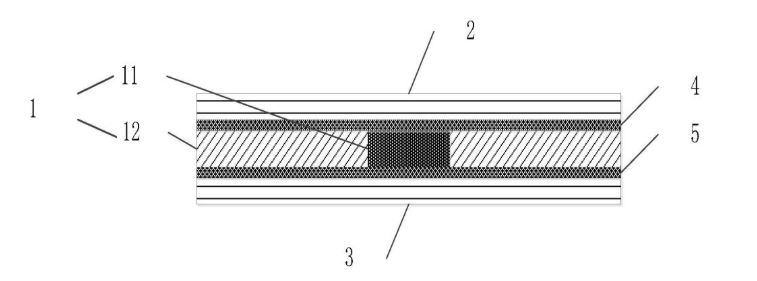
The core innovation of this patent is to achieve reliable connection between the copper-diamond composite layer and the upper and lower metal layers through the solder layer. The sandwich structure prepared by the traditional process using the pre-pressing and sintering process has the defect of insufficient interface bonding strength , while Huawei uses a metal frame structure to encapsulate the diamond particles and forms a metallurgical bond through the solder layer. This structural design not only retains the high thermal conductivity of copper (385W/m· K) and the low ( 1-2ppm /K) , but also improves the mechanical stability of the overall structure through interface strengthening .
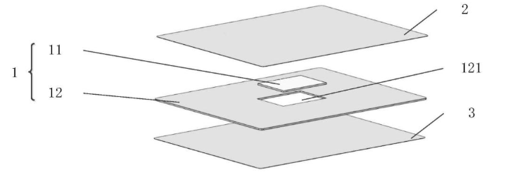
From the perspective of material composition, the copper-diamond composite layer is used as the core heat dissipation layer, and the metal layers above and below may use different material combinations. The first metal layer may use high thermal conductivity copper, and the second metal layer may use nickel alloy with better weldability . This gradient material design not only meets the heat conduction requirements , but also solves the interface stress problem of heterogeneous materials.
The core innovation of this patent is to achieve reliable connection between the copper-diamond composite layer and the upper and lower metal layers through the solder layer. The sandwich structure prepared by the traditional process using the pre-pressing and sintering process has the defect of insufficient interface bonding strength , while Huawei uses a metal frame structure to encapsulate the diamond particles and forms a metallurgical bond through the solder layer. This structural design not only retains the high thermal conductivity of copper (385W/m· K) and the low ( 1-2ppm /K) , but also improves the mechanical stability of the overall structure through interface strengthening .
From the perspective of material composition, the copper-diamond composite layer is used as the core heat dissipation layer, and the metal layers above and below may use different material combinations. The first metal layer may use high thermal conductivity copper, and the second metal layer may use nickel alloy with better weldability . This gradient material design not only meets the heat conduction requirements , but also solves the interface stress problem of heterogeneous materials.
Pretty smart. This will lead to faster clocked chips.
They should also consider backside power delivery to increase chip transistor density. And smaller SRAM cells like the 6T cells TSMC has that are used in the AMD dense server Ryzen 4c CPUs. This will allow more of the area to be devoted to logic.
They should also consider backside power delivery to increase chip transistor density. And smaller SRAM cells like the 6T cells TSMC has that are used in the AMD dense server Ryzen 4c CPUs. This will allow more of the area to be devoted to logic.
Last edited:
Fudan University and Fudan Microelectronics Group signed a strategic cooperation agreement to promote the upgrading of the integrated circuit industry
In the 27th anniversary of the establishment of Fudan Microelectronics Group, the "Independent Chip and Collaborative Approach" high-end forum was held at the Jiangwan Campus of Fudan University. During the forum, Fudan University and Fudan Microelectronics Group formally signed a strategic cooperation agreement, marking a new stage of in-depth cooperation between the two parties in key areas such as scientific research collaboration, technology transformation, and mechanism co-construction.
According to the agreement, the two parties will build a systematic cooperation framework around the three major directions of "platform co-construction - scientific research - talent collaboration", relying on Fudan University's research foundation and talent advantages in the field of integrated circuits, focusing on basic research, key technology research and engineering verification, and jointly promote scientific and technological achievements from the "paper stage" to the "application scenario", and open up the collaborative chain of industry, academia and research.
The agreement also clearly establishes a special mechanism to support the establishment of joint teams, sharing of experimental resources and coordinated promotion of projects, so as to enhance the engineering capabilities of university scientific and technological achievements and the innovation efficiency of enterprises.