Chinese semiconductor thread II

tokenanalyst

Brigadier
Registered Member

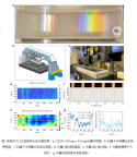
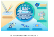
Progress in research on large-aperture grating diffraction wavefront control.​


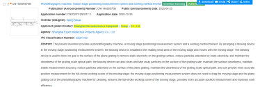
The research team of Bayinhexige and Li Wenhao from the National Grating Manufacturing and Application Engineering Technology Research Center of the Changchun Institute of Optics, Fine Mechanics and Physics, Chinese Academy of Sciences has made progress in the control of large-aperture grating diffraction wavefront.

Diffraction gratings can separate complex colors of light through periodic structures, and therefore are widely used in spectral analysis and wavefront control. The diffraction wavefront error will cause the performance of high-end instruments and equipment to deteriorate. In inertial confinement nuclear fusion, the grating diffraction wavefront error causes the laser beam combination wavefront distortion, affecting the quality of ultra-intense pulsed lasers; in astronomical spectrometers, the grating diffraction wavefront error will reduce the spectral resolution and detection sensitivity; in CNC machine tool displacement measurement systems, the grating diffraction wavefront error directly affects the displacement measurement accuracy. Therefore, the high-precision control of large-aperture grating diffraction wavefronts has become a core problem restricting the development of high-end instruments and equipment.
1745971117986.png1745971139905.png

The outstanding advantage of the scanning interference field exposure technology is that the phase of the interference fringe can be actively controlled in real time, and a grating with extremely small diffraction wavefront error can be produced. The principle is that two laser beams are superimposed at their beam waists to form a millimeter-diameter interference field on the grating surface, and the workbench performs two-dimensional step scanning motion for exposure. Therefore, the accuracy of the workbench displacement measurement directly determines the accuracy of the grating diffraction wavefront. However, traditional laser interferometry is easily affected by ambient temperature, humidity and pressure, and the displacement measurement accuracy of the workbench is reduced. To solve the above problems, the research team proposed a grating-laser complementary workbench displacement measurement technology, which uses a grating interferometer that is less affected by environmental factors at the far end for long-distance measurement, and a laser interferometer for short-distance measurement at the near end, thereby solving the contradiction between the range and accuracy of the workbench displacement measurement, and the repeatability accuracy of the workbench measurement reaches ±6nm. The research team also established a nanometer-precision interference field parameter measurement system. Through two sets of measurement systems, the displacement error of the workbench and the phase distribution of the exposure beam can be accurately obtained, and the dynamic phase control system is used to modulate the phase distribution of the interference fringes to achieve accurate phase splicing of adjacent interference fringes. This method can compensate for the grating line error caused by the worktable motion error and achieve high-precision production of large-aperture gratings.

Please, Log in or Register to view URLs content!
 

gotodistance

New Member
Registered Member
Korean professor believes Chinese HBM could be three years behind industry leaders, instead of the commonly assumed ten. Credits domestic R&D efforts to overcome sanctions.


This is the source of the Korean media
Please, Log in or Register to view URLs content!


- 한·중 HBM 격차가 10년 수준이라고 하는데, 중국 HBM은 어느 정도 수준인가.
△우리 생각보다 그게(큰 격차가) 아닐 수 있다. 중국은 상향 평준화가 많이 됐다. 일각에서는 3~4년밖에 격차가 나지 않는다고 한다.

- They say the HBM gap between Korea and China is about 10 years, but what is the level of China's HBM?
△ It may not be as big (a big gap) as we think. China has been leveled up a lot. Some say the gap is only 3-4 years.


======================================================
Apart from this news, do you trust the news from the Korean media? I don't trust the news about China from the Korean trash media. Most of it is fake news.
 

tokenanalyst

Brigadier
Registered Member

Lingang announces the design plan of Xinsheng Semiconductor's 300mm silicon wafer project​


On April 30, 2025, the Lingang Management Committee announced the design plan of Shanghai Xinsheng Semiconductor Technology Co., Ltd.'s "300mm silicon wafer research and development and industrialization project for integrated circuit manufacturing, and integrated circuit silicon material engineering research and development supporting project."

The project construction site is located in Nicheng Town, Pudong New Area. The boundaries are Plot 101-07 in the east, Plot I01-06 in the south, the green belt on the east side of Yunshui Road in the west, and the green belt on the south side of Laolitang River in the north.
Shanghai Xinsheng Semiconductor Technology Co., Ltd. is a wholly-owned subsidiary of Shanghai Silicon Industry Group Co., Ltd. and is a company that commercializes 300mm (12-inch) semiconductor silicon wafers. The 300mm silicon wafers produced by the company are widely used in integrated circuit industries such as memory chips, logic chips, image sensors, IGBT power devices and communication chips.

Integrated circuits are the leading industry with the largest investment scale, the highest industrial concentration, and the fastest output value growth in the Lingang New Area. The industry scale is expected to exceed 40 billion yuan in 2024 from less than 1 billion yuan in 2019, and the total industry scale target in the next three years is to strive to achieve 80 billion yuan.

Please, Log in or Register to view URLs content!
 

tokenanalyst

Brigadier
Registered Member

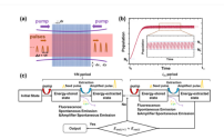
Theoretical analysis on gain and thermal performance of Tm:YLF-based 10 kW-level laser amplifier​

Abstract​

Recent advances in 2 μm laser technology demonstrate significant potential to replace conventional 10.6 μm lasers for generating efficient extreme ultraviolet (EUV) light sources. The multi-pulse extraction (MPE) technique, synergized with gain media exhibiting long fluorescence lifetimes (e.g., Tm:YLF), presents a viable strategy for achieving high-average-power 2 μm lasers. However, achieving kW-level average power output at 2 μm remains an area requiring further exploration. To investigate this, we propose potential technical pathways through comprehensive theoretical analyses of gain performance and thermal effects in Tm:YLF amplifiers. The gain performance model derived from laser rate equations and finite element analysis (FEA) simulations can further reveal temperature and thermal stress distributions in the crystals. These theoretical results exhibit excellent agreement with reported experimental data. Our results indicate that Tm:YLF is a suitable candidate for developing 2μm laser systems with high repetition rates and high average power (>10 kW). We also highlight critical technical challenges requiring further experimental validation, including thermal management optimization and MPE efficiency enhancement.

1746027662406.png

Please, Log in or Register to view URLs content!
 

tokenanalyst

Brigadier
Registered Member
1746029477756.png


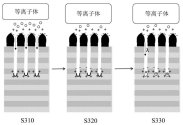
A pulsed plasma etching method combined with timed auxiliary light to enhance ion neutralization and by-product management:
  1. Dual-Stage Pulsed RF Cycles
    • First Stage (5–50% of pulse period):
      • High-frequency RF (>3 kW) + low-frequency RF (>10 kW) generate plasma for aggressive etching.
      • Forms deep recessed structures (e.g., 128-layer 3D NAND).
    • Second Stage (50–95% of pulse period):
      • RF Power Reduced: High RF (0–2 kW) + low RF (optional off).
      • Auxiliary Light Activated: UV light (<380 nm) enhances electron energy and by-product mobility.
      • Neutralizes residual ions and improves by-product distribution.
  2. Timed Light Activation
    • Light source triggered simultaneously (0s delay) or after a preset delay (10–30% of pulse period) to optimize charge neutralization.
    • Asynchronous dual-wavelength UV light (different stages) for targeted ion/electron dynamics.
  3. Adaptive Process Control
    • Variable Timing Stages: Process parameters (gas flow, pressure, RF power) adjusted across sequential etch stages to match depth-dependent requirements.
    • Pulse Period Range: 500 µs–10 ms for precise cycle management.
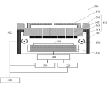
  4. Plasma Processing Device
    • Components:
      • Vacuum reaction chamber with substrate holder.
      • High/low RF power sources.
      • Circumferential UV light sources (≥2 wavelengths, <380 nm).
      • Controller for synchronized RF/light timing.
  • Improved Etch Uniformity: Reduces positive ion accumulation at structure bottoms, preventing sidewall distortion.
  • Enhanced By-Product Management: Light-driven photon absorption boosts by-product mobility, ensuring uniform distribution.
  • High-Aspect-Ratio Capability: Enables recessed structures with aspect ratios ≥50, critical for 128+ layer 3D NAND.
  • Yield Improvement: Reduces defects in self-aligned multi-patterning processes, enhancing device reliability.
  • Scalability: Adjustable parameters and multi-wavelength light sources adapt to evolving semiconductor node requirements.
1746029281802.png1746029313024.png
 

tokenanalyst

Brigadier
Registered Member

Extreme Ultraviolet Multilayer Defect Profile Parameters Reconstruction via Transfer Learning with Fine-Tuned VGG-16​

Abstract​

Extracting defect profile parameters from measured defect images poses a significant challenge in extreme ultraviolet (EUV) multilayer defect metrologies, because these parameters are crucial for assessing defect printing behavior and determining appropriate repair strategies. This paper proposes to reconstruct defect profile parameters from reflected field intensity images of a phase defect assisted by transfer learning with fine-tuning. These images are generated through simulations using the rigorous finite-difference time-domain (FDTD) method. The VGG-16 pre-trained model, known for its robust feature extraction capability, is adopted and fine-tuned to map the intensity images to the defect profile parameters. The results demonstrate that the proposed approach accurately reconstructs multilayer defect profile parameters, thus providing important information for mask repair strategies.

1746030591867.png

Please, Log in or Register to view URLs content!
 

tokenanalyst

Brigadier
Registered Member

Changdian Technology's revenue in the first quarter of 2025 increased by 36.4% year-on-year and hit a record high for the same period, and its net profit attributable to shareholders increased by 50.4% year-on-year​

Financial highlights for the first quarter of 2025:
  • The company achieved revenue of RMB 9.34 billion in the first quarter, a year-on-year increase of 36.4%, setting a record high for the same period in history.
  • The net profit attributable to shareholders of the parent company in the first quarter was RMB 200 million, a year-on-year increase of 50.4%.​
  • Net cash flow from operating activities in the first quarter was RMB 1.14 billion.​
  • Earnings per share were RMB 0.11 in the first quarter, compared with RMB 0.08 in the first quarter of 2024.​

April 28, 2025, Shanghai, China - Today, Changdian Technology (600584.SH), a global leading integrated circuit finished product manufacturing and technology service provider, announced its first quarter report for 2025. The report shows that the company achieved operating income of RMB 9.34 billion in the first quarter of 2025, a year-on-year increase of 36.4%, a record high for the same period in history; and achieved a net profit of RMB 200 million attributable to shareholders of listed companies, a year-on-year increase of 50.4%.

Since 2025, Changdian Technology has maintained a good momentum of steady progress and quality improvement in its business development, continued to focus on cutting-edge technologies and key application markets, further optimized its business structure, and further improved its domestic and overseas production capacity allocation and supply chain layout. During the reporting period, all businesses achieved significant year-on-year growth; in the field of computing electronics, the company provided high-performance chip finished product manufacturing solutions to global customers to meet the growing market demand, with revenue increasing by 92.9% year-on-year; the automotive electronics business further strengthened its one-stop service capabilities, with related revenue increasing by 66.0% year-on-year; the industrial and medical electronics business segment, revenue increased by 45.8% year-on-year. The company will adhere to the construction of a diversified, resilient and sustainable supply chain, pay close attention to the development of the international trade situation, continue to evaluate and respond to possible impacts, and maintain close communication with customers and suppliers.

With its leading comprehensive strength, Changdian Technology has further consolidated its position as a global leader in semiconductor packaging and testing, and was included in the "Top 30 Global Semiconductor Brand Value in 2025" list released by brand evaluation consulting agency Brand Finance in the first quarter of this year.

Under the guidance of the company's strategy, Changdian Technology will continue to promote lean production, optimize product structure and production capacity layout, and improve mid- and long-term profitability through technological upgrades and economies of scale.

Please, Log in or Register to view URLs content!
 

tokenanalyst

Brigadier
Registered Member

Huahai Qingke’s annual report released! Revenue of 3.406 billion yuan!​


Huahai Qingke released its 2024 annual report, which pointed out that in 2024, the company's operating income increased by 35.82% year-on-year to 3.406 billion yuan, and its net profit attributable to the parent company increased by 41.40% year-on-year to 1.023 billion yuan, and its net profit attributable to the parent company increased by 40.79% year-on-year to 856 million yuan. At the end of the reporting period, the net assets attributable to shareholders of the listed company increased by 17.31% from the end of the previous year, and the total assets increased by 28.88% from the end of the previous year, mainly due to the company's profit and inventory increase.

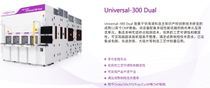
Huahai Qingke Co., Ltd. (hereinafter referred to as "Huahai Qingke") is a high-end semiconductor equipment manufacturer with core independent intellectual property rights. The company's main products include CMP equipment, thinning equipment, dicing equipment, wet equipment, ion implantation equipment, edge polishing equipment, round regeneration, key consumables and maintenance services, creating a platform-based strategic layout of "equipment + service". The company's main products and services have been widely used in integrated circuits, advanced packaging, large silicon wafers, third-generation semiconductors, MEMS, Micro LED and other manufacturing processes.

1746031100431.png

Please, Log in or Register to view URLs content!
 
Top