Chinese semiconductor thread II

tokenanalyst

Brigadier
Registered Member

The Institute of Semiconductors has made important progress in two-dimensional array lasers​


Vertical cavity surface emitting laser (VCSEL) is widely used in many fields such as pump source, consumer electronics, 3D sensing, medical beauty, etc. due to its advantages of low threshold, circular spot, single longitudinal mode, low temperature drift coefficient, high reliability and easy two-dimensional integration. However, traditional VCSEL has certain limitations in output power. In order to increase the power, methods such as increasing the oxidation aperture, multi-junction structure and expanding the array scale are usually adopted. Although these methods can increase the output power, they lead to problems such as increased divergence angle and transformation of transverse mode into high-order mode, which in turn reduces the beam quality (Beam Parameter Product, BPP), and ultimately leads to a sharp decrease in brightness. Therefore, the constraint between high power and high beam quality has become one of the core problems in the development of VCSEL technology, and has greatly limited its application in remote detection and lighting systems that require high-brightness light sources such as lidar and space optical communications.


To solve this bottleneck, the team of Academician Zheng Wanhua from the Solid-State Optoelectronic Information Technology Laboratory of the Institute of Semiconductors, Chinese Academy of Sciences, and other institutions, together with the University of Chinese Academy of Sciences , innovatively proposed a two-dimensional solid-state laser array (SSLA) solution. This technology directly integrates a large-size high-power VCSEL array with a thin Nd:YVO 4 laser crystal to construct a compact two-dimensional array laser structure, which can significantly improve the beam quality while achieving proportional power expansion. Experimental data show that this 3×3 mm 2 SSLA array has a single pulse energy of 4.7 mJ at a central wavelength of 1 μm, an optical-to-optical conversion efficiency of 52%, and a surface light source brightness of up to 1.27 kW·cm -2 ·sr -1 , which is nearly three orders of magnitude higher than the traditional VCSEL array.
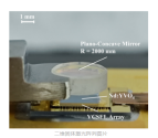
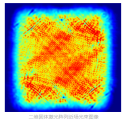
1745935841529.png1745935851126.png

Its innovation is reflected in: ① Each light-emitting unit maintains an excellent beam quality of M 2 <1.5; ② Inherits the inherent laser emission array mode of the VCSEL array; ③ Breaks through the traditional contradiction between power expansion and beam degradation. This "high power-high brightness-high integration" trinity technological breakthrough provides a lightweight, high-brightness light source solution for long-range detection systems. In addition, this breakthrough in two-dimensional solid-state laser array technology not only opens up new possibilities for the further development of traditional application fields, but also lays a technical foundation for applications in emerging fields such as high-speed data transmission, three-dimensional imaging, and precision ranging. In the future, as technology continues to mature, the chip-based design of planar array laser sources will become an important direction for the development of laser technology, pushing laser technology towards a more efficient and compact future.

Please, Log in or Register to view URLs content!
 

tokenanalyst

Brigadier
Registered Member

Standard | Huafeng Testing and Control led the drafting of three SiC MOSFET UIS/single-tube short-circuit/module short-circuit test methods for comments​

Three SiC MOSFET technical standards drafted by Beijing Huafeng Measurement & Control Technology Co., Ltd. have completed the preparation of the draft for comments and are officially oriented to the third-generation semiconductor
On April 29, 2025, the three SiC MOSFET technical standards drafted by Beijing Huafeng Measurement & Control Technology Co., Ltd. have completed the preparation of the draft for comments and formally solicited opinions from the member units of the Third Generation Semiconductor Industry Technology Innovation Strategic Alliance for a period of one month. According to the Alliance Standardization Management Measures, comments will be solicited from April 29, 2025, and the deadline is May 29, 2025.

T/CASAS 038—202X "SiC MOSFET Unclamped Inductive Switching (UIS) Test Method"


This document specifies the test method for SiC MOSFET Unclamped Inductive Switch (UIS), including the test principle, test process, data recording and processing of single pulse avalanche breakdown energy (EAS) and repetitive avalanche breakdown energy (EAR).

This document is applicable to UIS testing of SiC MOSFET discrete devices in the FT (Final Test), CP (Chip Probe), KGD (Known Good Die), laboratory research and development stages. For SiC MOSFET power modules, this document can be used to test a single tube before packaging it into a module.

T/CASAS 039—202X " Short-circuit reliability test method for SiC MOSFET single-tube power devices "

This document specifies the test method for the short-circuit reliability of SiC MOSFET single-tube power devices, including the test principle, test process, data recording and processing of Class I, Class II and Class III short circuits.

This document is applicable to the short-circuit reliability test of SiC MOSFET single-tube power devices in the FT (Final Test), CP (Chip Probe), KGD (Known Good Die), laboratory research and development stages.

T/CASAS 040—202X "SiC MOSFET power module short circuit reliability test method"

This document specifies the short-circuit reliability test method for SiC MOSFET power modules, including test principles, test procedures, data recording and processing, etc.

This document is applicable to the short-circuit reliability test of SiC MOSFET power modules in the FT (Final Test) and laboratory R&D stages.

Please, Log in or Register to view URLs content!
 

tokenanalyst

Brigadier
Registered Member

Chip-level diamond packaging substrate manufacturing headquarters project signed!​


The chip-level diamond packaging substrate manufacturing headquarters project was signed and settled in Jiangyin Xiakewan Science City, injecting strong momentum into Jiangyin's efforts to accelerate the cultivation of new quality productivity and enhance the support for the development of the integrated circuit industry. Xu Feng, member of the Wuxi Municipal Party Committee and Secretary of the Jiangyin Municipal Party Committee, attended the signing ceremony and held talks with Li Huaguo, Chairman of Huatai International Energy Development Co., Ltd.

Please, Log in or Register to view URLs content!
 

tokenanalyst

Brigadier
Registered Member

Lianke Semiconductor's eight-inch silicon zone furnace and silicon carbide resistance furnace have reached the international leading level.​

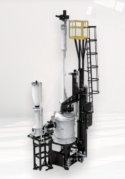
8-inch/12-inch silicon carbide resistance furnace and process technology package" project, in collaboration with Zhejiang University and other institutions, was the first in the industry to introduce a DC dual-power heater and a dual-temperature zone thermal field structure, with a 35% drop in heating power to 28Kw; high-precision control software was developed to achieve precise control of gas flow and pressure, meeting the requirements for the stable growth of 8-inch/12-inch SiC single crystals, with high technical difficulty and complexity. After being promoted and applied by a number of silicon carbide substrate companies, it has achieved significant economic and social benefits, helping customers grow 8-inch/12-inch silicon carbide crystals with a thickness of more than 5cm. The overall technology of the project has reached the international leading level.

The "200mm Zone Floating Silicon Single Crystal Furnace Complete Technology" project has created a unique technology in which the lower spindle and the sealing liner are driven by servo motors and synchronously coupled and controlled, and a new control idea of the second camera measuring the melt flow, which has overcome the problems of high-precision processing and assembly of the spindle. A full-chain technology system of key technology-prototype demonstration-industrial application has been formed. The technology is difficult and complex. The project technology has been successfully put into production and stably operated at Youyan Semiconductor Silicon Materials Co., Ltd., with good technical reproducibility and high maturity. The overall technology of the project has reached the international leading level.

1745941886676.png

Please, Log in or Register to view URLs content!
 

tokenanalyst

Brigadier
Registered Member

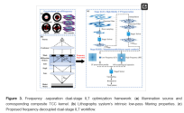
Frequency-Decoupled Dual-Stage Inverse Lithography Optimization via Hierarchical Sampling and Morphological Enhancement​

Abstract​

Inverse lithography technology (ILT) plays a pivotal role in advanced semiconductor manufacturing because it enables pixel-level mask modifications, significantly enhances pattern fidelity, and expands process windows. However, traditional gradient-based ILT methods often struggle with the trade-off between imaging fidelity and mask manufacturability due to coupled optimization objectives. We propose a frequency-separated dual-stage optimization framework (FD-ILT) that strategically decouples these conflicting objectives by exploiting the inherent low-pass characteristics of lithographic systems. The first stage optimizes low-frequency (LF) components using hierarchical downsampling to generate a high-fidelity continuous transmission mask. This approach reduces computational complexity while refining resolution progressively. The second stage enforces manufacturability by exclusively adjusting high-frequency (HF) features through morphological regularization and progressive binarization penalties while maintaining the mask LF to preserve imaging accuracy. Our method achieves simultaneous control of both aspects by eliminating gradient conflicts between fidelity and manufacturing constraints. The simulation results demonstrate that FD-ILT achieves superior imaging quality and manufacturability compared to conventional gradient-based ILT methods, offering a scalable solution for advanced semiconductor nodes.​

1745959722463.png

Please, Log in or Register to view URLs content!
 

tokenanalyst

Brigadier
Registered Member
Cool stuff.

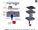
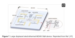
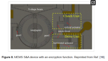
Application Prospects of a Silicon-Based MEMS Safety and Arming Device for a Micro-Explosive Train​


Abstract​

As the initial energetic device and driving force of weapon systems, pyrotechnics serve as the core and most sensitive explosive initiating device of weaponry. To accommodate the development requirements of various informatized and miniaturized weapons, MEMS pyrotechnics, characterized primarily by energy conversion informatization, structural miniaturization, and train integration, have become a significant direction in the development of pyrotechnics technology. MEMS Safety and Arming Devices, serving as the energy transfer control mechanisms for micro-explosive trains in MEMS pyrotechnics, are one of the key technologies in the design of MEMS pyrotechnics. This study conducted a classification study of a silicon-based MEMS Safety and Arming Device from the perspective of micro-explosive train structures, analyzed the technical principles of different S&A device, explored their application progress and research status, and summarizes the trends of the micro-miniaturization, integration, and informatization of the silicon-based MEMS Safety and Arming Device, providing new ideas for the research and the design of MEMS Safety and Arming Devices.​

1745960008655.png1745960056948.png
1745960082534.png

Please, Log in or Register to view URLs content!
 

tokenanalyst

Brigadier
Registered Member

Microelectronics Institute makes progress in carbon-silicon three-dimensional heterogeneous integrated devices​

As the density of integrated circuits continues to increase, the process nodes of transistors continue to shrink and are approaching physical limits. Three-dimensional complementary field-effect transistor (3D CMOS) technology has become a potential path to break the deadlock. Traditional silicon-based 3D CMOS integration technology has a high thermal budget, which leads to complex processes and increased costs, and may cause performance degradation and other problems, limiting its commercial application.

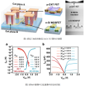
In response to the above problems, the team led by Li Bo, a researcher, and Lu Peng, an associate researcher at the Radiation Resistance Laboratory of the Institute of Microelectronics, Chinese Academy of Sciences, proposed a 3D CMOS technology of carbon nanotube/silicon heterogeneous integration (CNT/Si Heterogeneous Integration) based on the low-temperature film formation capability of carbon nanotube materials, and realized the low-temperature (≤150℃) carbon nanotube device integration of 180nm SOI devices. The team proposed a process optimization solution for high-performance digital circuit applications, achieved precise control of the threshold voltage of carbon nanotube devices, and was able to match the electrical characteristics of N and P transistors. The 3D CMOS noise margin was significantly improved (NM H /NM L  = 0.404/0.353× V DD ), while achieving excellent performance such as high gain (~49.9), ultra-low power consumption (390 pW) and high uniformity (chip-to-chip variation <6%). To demonstrate the integration capability of this technology in advanced process nodes, the team used TCAD simulation to build a 14nm FinFET/CNT 3D CMOS circuit unit. Theoretical analysis showed that it outperformed the commercial 14nm-FinFET process in terms of noise tolerance and power consumption.

1745970928762.png


The paper based on this research result, "Low-Thermal-Budget Construction of Carbon Nanotube p-FET on Silicon n-FET toward 3D CMOS FET Circuits with High Noise Margins and Ultra-Low Power Consumption", was recently published in the internationally renowned journal Advanced Functional Materials (DOI: 10.1002/adfm.202504068). This work was completed by the research team of Li Bo from the Institute of Microelectronics, the research team of Zhu Maguang from Nanjing University, and the team of Professor Hu Haibo from Anhui University, with the Institute of Microelectronics as the first unit. 

Please, Log in or Register to view URLs content!
 
Top