Chinese semiconductor thread II

tphuang

General
Staff member
Super Moderator
VIP Professional
Registered Member

TSMC apparently responded to reports of supplying AI chips to Huawei​


A new report says that
Please, Log in or Register to view URLs content!
has finally broken its silence and responded to the ‘Huawei AI chips’ controversy. After months of investigation, the chip producer has come up with its answers, denying allegations that it helped the Chinese company.

Please, Log in or Register to view URLs content!
that kind of article doesn't matter. TSMC told commerce department that they fabb'd 3 million die for Huawei.

There are actual photos of teardown and examinations Ascend-910C using TSMC process.
 

tokenanalyst

Brigadier
Registered Member

Hesai's 1440-line automotive-grade ultra-high-definition LiDAR is expected to be mass-produced in the second half of the year​


According to the "Science and Technology Innovation Board Daily" on the 21st, Hesai Technology today released the "Thousand-Li Eye", a laser radar perception solution for L2 to L4, and released a new generation of automotive-grade laser radar products, including the ETX automotive-grade ultra-long-range laser radar, the AT1440 automotive-grade ultra-high-definition laser radar, and the FTX automotive-grade pure solid-state blind laser radar. Among them, the AT1440 has 1,440 lines and a point frequency of more than 34 million points per second. The product will start mass production in the second half of 2025 and will be launched on Carl Power's first future transportation robot in the world. In an interview with reporters from the "Science and Technology Innovation Board Daily" and other media, Hesai Technology CEO Li Yifan said that the price of laser radar is still decreasing this year, but sales are rising rapidly.

Please, Log in or Register to view URLs content!
 

tokenanalyst

Brigadier
Registered Member

Pure Semiconductor Launches 3rd Generation SiC MOSFET Product Platform​


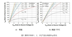
Recently, Pure Semiconductor launched the third-generation silicon carbide (SiC) MOSFET technology platform. The first main drive chip of this platform (model: S3M008120BK) has a room temperature on-resistance as low as 8mΩ. Through patented technology and process improvement, this platform has achieved a specific on-resistance coefficient Rsp = 2.1 mΩ.cm², which is leading among similar international products, as shown in Figure 1. It further achieves high current handling capability and lower loss, helping new energy vehicle motor drivers to further release the potential of SiC's high power density and high energy conversion efficiency, and improve driving range..

1745331895171.png
Please, Log in or Register to view URLs content!
 

tokenanalyst

Brigadier
Registered Member

Huayuan Optoelectronics received tens of millions of yuan in angel round financing to accelerate the development of semiconductor light sources​


Tianjin Huayuan Optoelectronics Technology Co., Ltd. recently completed an angel round of financing of tens of millions of yuan, jointly invested by Weihao Chuangxin and Changchang Investment. This round of financing will accelerate the verification and mass production of core products, and inject new momentum into the independent control of the semiconductor manufacturing industry chain.

Huayuan Optoelectronics is a high-end solid-state laser supplier. The technical team originated from the Department of Precision Instruments of Tsinghua University. It directly addresses the technical pain points of the industry and tackles the independent control of key light source technologies. Dr. Li Peilin, the founder and CEO, has been deeply involved in high-performance solid-state laser technology for more than 10 years and has led a number of national scientific research projects. He is committed to creating domestic high-end light sources with comparable performance to international standards and more competitive costs.

Faced with the dilemma of long-term reliance on overseas sources for high-end lasers, Huayuan Optoelectronics has achieved a leap from technology verification to industrialization through innovation in underlying technologies. With the start of production line construction, the company expects to start production within the year and plans to promote domestic substitution of semiconductor equipment light sources in the next three years to become a leading domestic supplier of high-end solid-state lasers.


Topazchen

Junior Member
Registered Member
More of a leverage, like what I said way way before, why destroy something you owned and why give your enemy the satisfaction. It's just what the American wanted, harvesting Taiwan and sucking the young blood out of them.
It's not leverage if you can't use it .
 

tokenanalyst

Brigadier
Registered Member

Perovskite equipment company Kaifu Optoelectronics completes angel round financing, led by Zhongke Chuangxing​


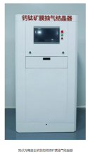
Recently, Kaifu Green Energy (Xi'an) Optoelectronics Co., Ltd. (hereinafter referred to as "Kaifu Optoelectronics"), an innovative enterprise specializing in the mass production of core equipment for efficient and stable perovskite solar cells, announced the completion of its angel round of financing. This round of financing was led by Zhongke Chuangxing and followed by Xi'an Talent Fund. The financing funds will be mainly used to accelerate the industrialization of the core product "perovskite film vacuum crystallizer", overcome the problems of uneven and incomplete solvent evaporation and poor film crystallization quality and many defects in the manufacturing process of large-area perovskite films, and solve the current bottleneck problems of low efficiency, low yield and short life of large-area perovskite modules in mass production.

Kaifu Optoelectronics was established in May 2023. The founding team focuses on large-area perovskite film vacuum crystallization technology and equipment, and took the lead in undertaking the first key project of common key technology in the national key R&D plan in the field of perovskite photovoltaics. Since 2014, it has cooperated deeply with a number of leading perovskite battery companies, verified the whole chain, and gradually realized the possibility of theory, feasibility of route, availability of technology, and reliability of equipment. It has developed a full-size series of perovskite film vacuum crystallizer equipment, including mass production equipment with a maximum area of 2400mm×1215mm, half-meter pilot equipment, and 30mm~210mm experimental equipment.

1745332608823.png

Please, Log in or Register to view URLs content!
 

tokenanalyst

Brigadier
Registered Member
Design Method of Microlens Arrays for Decoherence in Flexible Pupil Shaping Module

Abstract
Objective

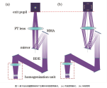
To further decrease lithographic resolution, specific illumination modes are required for different mask patterns. The freeform pupil-shaping module is a standard component of lithography illumination systems at the 28 nm node and below. To ensure stable and uniform energy distribution at the optical pupil, a homogenization unit is used before the freeform pupil-shaping module. The current mainstream solution involves using a microlens array (MLA) for homogenization. The MLA divides the incident beam into a multitude of sub-beams, which are superimposed on the back focal plane of the condenser to obtain a homogeneous illumination field. Although a low-spatial-coherence excimer laser is used in lithography, it still produces interference patterns in the back focal plane of the condenser, significantly impacting pupil performance. In this paper, we propose a decoherence method based on the deformation design of MLAs that improves the uniformity without introducing additional elements.
Methods
In this paper, we propose a new design method for decoherent MLAs. First, considering the partial coherence of a laser, transmission of partially coherent light in the homogenization unit is modeled using mutual intensity theory. Based on the mutual intensity distribution in the back focal plane of the condenser, it can be concluded that the intensity distribution of the light field is modulated by the coherence length and related to the aperture function P(?,η). Changing this function not only affects the initial phase φ(m,n) of each sub-beam but also changes the frequency of sinc function. As a consequence, φ(m,n) affects the interference results and sinc function affects the amplitude modulation. Based on the aforementioned model, an optimized design of the mean value of the pitch size of the MLA was carried out. To increase the phase difference between the microlenses within the coherence length, degrees of freedom for pitch variation and border line tilting were introduced based on the optimized design described above.
Results and Discussions
First, the mean value of the pitch size of the MLA was optimized. The design results (Figs. 5 and 6) show that when the microlens pitch size is 0.5 mm, non-uniformity is at a minimum of 43.87% and energy utilization is 85.39%. While this optimization solution satisfies the energy utilization requirement of the freeform pupil-shaping module, it is not able to achieve a non-uniformity less than 40%. Introducing a small random pitch variable in the pitch size of the microlens, the design results (Figs. 8 and 9) show that non-uniformity is minimum at 41.53% and energy utilization is 84.16% at the amplitude of the pitch variation of 0.05 mm, which also satisfies the requirement for energy utilization. However, non-uniformity does not fulfill the aforementioned requirement yet. Making the microlens at the cylindrical border line in the xy plane introduces a tilt factor k, which is a random small quantity. The design results (Figs. 11 and 12) show that when the amplitude of the tilt factor is 5 μm, non-uniformity is at a minimum of 38.67%, and energy utilization is 82.74%, thereby fulfilling specifications. Combining the optimization solutions of pitch size variation and border line tilting, non-uniformity of 36.51% (Fig. 14) and energy utilization of 83.90% are achieved when the amplitude of the pitch variation is 0.03 mm and that of the tilting factor is 4 μm. This co-optimization approach results in a more significant reduction in non-uniformity, along with improved energy utilization.​


1745335448477.png

Please, Log in or Register to view URLs content!
 

tokenanalyst

Brigadier
Registered Member

Kaishitong's low-energy, large-beam ion implanter's daily production capacity breaks a record high​

At the beginning of April, Kaishitong's low-energy, large-beam ion implanter achieved a major breakthrough on the production line of key customers. After breaking through the 2,400-piece mark, its product daily production capacity (24 hours) quickly broke through to 3,200 pieces, successfully achieving a milestone leap in the mass production of domestic ion implanters in advanced chip production lines, demonstrating the strong rise of domestic equipment in the field of high-end chip manufacturing.

The birth of this breakthrough is the result of the Kaishitong team's long-term efforts to improve CIP and continuously optimize the service system, reflecting the confidence and support of customers in Kaishitong's ion implanter equipment and on-site services. After continuous upgrades and iterations, Kaishitong's ion implanter has demonstrated excellent performance and stability on the client side, and has won high recognition from customers with its strong strength. With a high sense of responsibility and professionalism, Kaishitong's customer service team insists on providing customers with 7×24-hour all-weather and efficient services, promoting the continuous improvement of equipment performance and utilization, and injecting strong impetus into customers' safe production and cost reduction and efficiency improvement.

In the wave of domestic substitution of semiconductor equipment, Kaisitong will, as always, uphold the customer-centric development philosophy, work hand in hand with customers, and jointly write the "core" chapter for the development of domestic semiconductor industry.​

Please, Log in or Register to view URLs content!
 
Top