Chinese semiconductor thread II

tokenanalyst

Brigadier
Registered Member

Keyun Laser breaks the monopoly! Another equipment is localized and shipped​


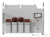
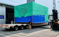
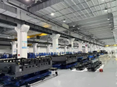
Recently, the first G11 ultra-large display panel laser patterning equipment independently developed by Suzhou Keyun Laser Technology Co., Ltd. was successfully shipped to the leading display panel factory in China. As the only company in China that can provide this equipment, Keyun Laser has broken the monopoly of Japanese and Korean equipment companies, which is of great significance for enhancing the autonomy of domestic precision laser equipment in the new display industry chain.

Following the first batch shipment of G8.6 generation display panel laser graphics equipment in 2023, Keyun Laser's shipped equipment this time corresponds to larger product sizes and higher processing precision requirements. This type of equipment was previously supplied by Japanese and Korean equipment manufacturers, and is mainly used for laser precision graphics marking of the film layer of the glass substrate of the G11 generation display panel. Keyun Laser's domestically produced G11 ultra-large size display panel laser graphics equipment covers an area of more than 30 square meters and weighs more than 40 tons. It adopts a large-size, high-precision integrated gantry structure with a gantry span of more than 5 meters, achieving an ultra-long span repeat positioning accuracy of ±1 micron; in terms of laser technology, the G11 generation line has achieved ultra-large format path splicing, and the laser graphics marking accuracy has reached ±10 microns; further breakthroughs have been made in the visual precision detection technology of deep visual images and learning fusion strategies, as well as the construction of AI intelligent algorithms, and the main technical indicators have reached international advanced and domestic leading levels.

The equipment is developed and manufactured in the new base factory of Keyun Laser. Currently, the new base factory is equipped with a 10,000-class clean workshop area of 30,000 square meters and a 10,000-class clean dust-free laboratory of 3,000 square meters, which can meet the production and manufacturing of 100 sets of laser precision equipment at the same time
1753214032386.png1753214082148.png

Please, Log in or Register to view URLs content!
 

interestedseal

Junior Member
Registered Member
长鑫存储于 2025 年 6 月完成12 层 HBM3 样品开发,通过国内 AI 芯片厂商测试认证,并与头部客户签署试点合同。其 TSV(硅通孔)堆叠良率达89%,接近SK 海力士 HBM3E 的 92% 水平,单堆栈容量达24GB,带宽突破800GB/s,性能对标三星 HBM3 Icebolt(819GB/s)。通过混合键合(Hybrid Bonding)专利优化散热设计,在 12 层堆叠架构下实现热阻降低 30%,超越 SK 海力士现有方案。
Please, Log in or Register to view URLs content!

Confirmation from their FC-BGA substrate supplier that CXMT 12-layer HBM3 samples are being delivered&tested (with good TSV yield) It’s really not a surprise since they started D1z mass production in 2024. Somewhat surprising that they skipped TCB and used hybrid bonding instead, which likely uses the Pleione hybrid bonder from Piotech
Please, Log in or Register to view URLs content!

Please, Log in or Register to view URLs content!
 

tphuang

General
Staff member
Super Moderator
VIP Professional
Registered Member
Please, Log in or Register to view URLs content!

Confirmation from their FC-BGA substrate supplier that CXMT 12-layer HBM3 samples are being delivered&tested (with good TSV yield) It’s really not a surprise since they started D1z mass production in 2024. Somewhat surprising that they skipped TCB and used hybrid bonding instead, which likely uses the Pleione hybrid bonder from Piotech
Please, Log in or Register to view URLs content!

Please, Log in or Register to view URLs content!
This is awesome news. I think they were rumored by the Korean media for a while so it’s good to see some report of this out of China.

also very interesting that it has already received orders and got validated. I would assume that’s for the next ascend chips but who knows.
 
Last edited:

JPaladin32

New Member
Registered Member
This is significant and should not be overlooked.

A score of 22/GHz is even higher than Apple M1. While Kirin X90 has already reached the level between Apple M2 and M3, that is multi-core and single-core is still 30% behind M1. If the numbers are true, the single-core performance of Kunminghu-V3 is now on-par with M1. This chip is a beast (assuming the numbers on the slides are legitimate).
 

tokenanalyst

Brigadier
Registered Member

TCL Electronics' first-half net profit is expected to increase by 45%-65%; Mini LED TV shipments surge 176%​

TCL Electronics released a profit forecast for its interim results for 2025, predicting that its adjusted net profit attributable to shareholders in the first half of the year will reach HK$950 million to HK$1.08 billion, a significant increase of 45% to 65% over the same period in 2024. The performance growth is mainly due to the deepening of its globalization strategy, technological breakthroughs in high-end products and improved supply chain efficiency, demonstrating the company's strong resilience in a complex market environment.

According to the disclosure, TCL Electronics continues to increase the research and development of high-end display technologies such as Mini LED to promote the upgrading of product structure. In the first half of 2025, the company's global TV shipments reached 13.46 million units, a year-on-year increase of 7.6%, and its market share remained in the top two in the world. Among them, Mini LED TV performed particularly well, with global shipments surging 176.1% year-on-year, ranking first in the industry. In addition, the global average shipment size of TCL TV increased to 53.4 inches, an increase of 1.5 inches year-on-year, and the implementation of the mid-to-high-end strategy has achieved remarkable results.

In the international market, TCL Electronics has effectively responded to changes in the trade environment through overseas production capacity layout in Mexico, Vietnam and other countries. In the first half of the year, overseas TV shipments increased by 8.7% year-on-year. In the Chinese market, TCL brand TV shipments increased by 10.2% year-on-year, and retail volume ranked first and second. The company became an Olympic global partner in early 2025, and its brand influence continued to expand, injecting new momentum into performance growth.

Please, Log in or Register to view URLs content!
 

tokenanalyst

Brigadier
Registered Member

Wushiwei's "12-inch ultra-thin wafer (20-30um) post-debonding cleaning machine" won the Jiangsu Province "Two New" technology products​

Recently, the Jiangsu Provincial Department of Industry and Information Technology announced the list of "three firsts and two new" technology products to be recognized in Jiangsu Province in 2025. A total of 1,846 products in the province were on the list. Among them, the technical product "Post-debonding cleaning machine for semiconductor 12-inch ultra-thin wafers (20-30um)" declared by our company is also on the public list.

With its unique protection design for fragile wafers, the cleaning equipment from Wushiwei is suitable for the processing of 8/12-inch ultra-thin wafers and plays a key role in multiple links of the semiconductor industry:
1. Wafer thinning and post-debonding cleaning (core scenario)
2. Cleaning with blue film protection: protect the blue film from being corroded by the solution, directionally clean the front side of the wafer to ensure cleanliness.
The equipment's "flexible protection + rigid constraint" design solves the contradiction between "vulnerability" and "high-precision cleaning requirements" when cleaning ultra-thin wafers, and will provide key support for high-end processes in the fields of 2.5D/3D packaging, MEMS chips, etc.

1753284205484.png

Please, Log in or Register to view URLs content!
 

tokenanalyst

Brigadier
Registered Member
SiC devices and EV electronics are going to get more cheaper​

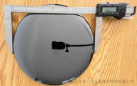
Jingyue Semiconductor has developed high-quality 12-inch SiC ingots​


After successfully mass-producing 8-inch silicon carbide substrates in the first half of 2025, Jingyue Semiconductor has continued to invest and increase its R&D efforts, and has continuously adjusted and optimized the process in thermal field design, seed crystal bonding, thickness improvement and defect control. On July 21, it developed a high-quality 12-inch SiC ingot, marking Jingyue's successful entry into the 12-inch SiC substrate echelon.

1753284489328.png

In the future, Jingyue will continue to invest in research and development, focus on polishing products, improving yield and parameter optimization, and strive to become a leading domestic silicon carbide material provider.

Please, Log in or Register to view URLs content!
 

tokenanalyst

Brigadier
Registered Member

Kema Technology: Plans to acquire 73% equity of Suzhou Kaixin Semiconductor for RMB 102 million​

Suzhou Kema Materials Technology Co., Ltd. (stock name: Kema Technology) issued an announcement that it plans to acquire 73.00% of the equity of Suzhou Kaixin Semiconductor Technology Co., Ltd. (hereinafter referred to as "Suzhou Kaixin") with RMB 102.3702 million in cash. After the completion of this transaction, it will directly hold 73.00% of the equity of Suzhou Kaixin.

The announcement shows that Suzhou Kaixin is a high-tech enterprise engaged in the research, development, production and sales of chemical vapor deposition (CVD) silicon carbide coatings and CVD silicon carbide bulk ceramic components. Relying on independent research and development, the company has rich accumulation and continuous research and development capabilities in the technologies and processes related to CVD silicon carbide ceramic components. At present, its products have been applied on a large scale in the fields of Si epitaxy, SiC epitaxy, GaN epitaxy, etc., and the development of advanced products such as silicon carbide etching rings, silicon carbide shower heads, and 12-inch Si epitaxy silicon carbide coated graphite bases has made good progress.
1753284749337.png

Suzhou Kaixin's product layout and R&D capabilities in the field of silicon carbide ceramics are highly complementary to Kema Technology's existing product system. This acquisition will help Kema Technology further enrich and improve its product layout in the field of silicon carbide ceramic materials and components, forming a more comprehensive and complete silicon carbide material system and semiconductor ceramic component system, which will help further improve the comprehensive service capabilities for semiconductor customers, while also further expanding the application of Kema Technology's silicon carbide material system in other national economic fields.

Please, Log in or Register to view URLs content!
 

snake070

New Member
Registered Member
Piezoelectric High Temperature Liquid Droplet Spraying Component

(1. University of Chinese Academy of Sciences, Beijing 100049, China; 2. Shanghai Institute of Ceramics, Chinese Academy of Sciences, Shanghai 200050, China; 3. Shanghai Institute of Optics and Fine Mechanics, Chinese Academy of Sciences, Shanghai 201800, China)

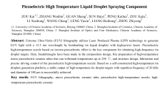
Abstract: Extreme Ultra-Violet (EUV) lithography utilizes Laser Produced Plasma (LPP) technology to generate EUV light with a 13.5 nm wavelength by bombarding tin liquid droplets with high-power lasers. Piezoelectric high-temperature nozzle based on inverse-piezoelectric effect is the key component for obtaining high-frequency tin droplet targets. Here, breakthroughs have been made in the composition design, fine preparation of high-temperature micro piezoelectric ceramic tubes that can withstand temperatures up to 250 ℃, and structure design, fabrication and precise driving control of the piezoelectric high-temperature nozzle. Based on a self-constructed high-temperature tin droplets generation platform, a stable output of high-temperature tin droplet targets with repetition frequency of 20 kHz and diameter of 100 μm is successfully achieved. Key words: EUV lithography; micro piezoelectric ceramic tube; piezoelectric high-temperature nozzle; high- temperature piezoelectric ceramic

滴吧原件.png

Please, Log in or Register to view URLs content!
 
Top