You are using an out of date browser. It may not display this or other websites correctly.
You should upgrade or use an alternative browser.
You should upgrade or use an alternative browser.
Chinese semiconductor thread II
- Thread starter vincent
- Start date
Chinese researchers use "softness to overcome hardness" to fill the gap in non-destructive testing technology for micro LED wafers
Chinese research team has developed a contact-based, non-destructive method for micro-LED wafer testing, addressing a longstanding challenge in electroluminescence inspection of micro-LED technology.
The soft-contact approach uses a flexible three-dimensional probe array capable of adapting to the microscopic contours of micro-LED wafers, applying pressure as low as 0.9 megapascals -- comparable to the softness of a gentle breath and just one ten-thousandth that of conventional rigid probes.
Jingsheng Electromechanical's subsidiary Qiushi Chuangxin's 12-inch equipment was successfully delivered
Recently, the 12-inch atmospheric pressure silicon epitaxial equipment independently developed by Zhejiang Qiushi Chuangxin Semiconductor Equipment Co., Ltd., a subsidiary of Jingsheng Electromechanical , was successfully delivered to a leading domestic customer.
The 12-inch atmospheric pressure silicon epitaxial equipment delivered this time is based on chemical vapor deposition technology. It can epitaxially grow a complete single crystal layer with consistent crystal orientation and adjustable parameters on a single crystal silicon substrate with a specific crystal orientation. Its key indicators such as resistivity, thickness uniformity, epitaxial layer defect density, production efficiency and process repeatability have reached the international advanced level . In addition, the equipment also has outstanding advantages in delivery cycle, service response and customized development, effectively helping customers reduce production costs and ensure supply chain security, thereby establishing long-term and differentiated competitive advantages.
With the rapid rise of emerging industries such as new energy vehicles, 5G communications, and the Internet of Things, the demand for high-performance silicon epitaxial wafers has increased dramatically, and higher requirements have been placed on the technical level of epitaxial growth equipment. Qiushi Chuangxin's successful delivery this time will provide domestic customers with more competitive equipment options.

Last edited:
Chongqing Wanzhou has built a base for the entire industrial chain of compound semiconductor chips
On June 10, the compound semiconductor chip packaging module production line of Vecosele Microelectronics Co., Ltd. in Wanzhou, Chongqing, was officially put into mass production, successfully opening up the entire chain from key raw material extraction, core chip manufacturing to high-end packaging modules, and taking the lead in building a compound semiconductor chip full industry chain base in the country.
"Chip packaging is like putting on a solid armor for the bare die, providing electrical signal connection, heat dissipation and protection." said Quan Benqing, director of the new business department of Vicosele Microelectronics Co., Ltd. After packaging, the bare die becomes a single-chip device with independent functions. The packaging module integrates multiple such single-chip devices in the package body like building blocks, forming a system-level solution with more complex functions and stronger performance.
At present, Vicosele has a full range of GaAs-based chip products. "With the commissioning of the packaging module production line, we can design and manufacture compound semiconductor chips and complete system-level integration without relying on external resources, and have the complete delivery capability from materials to terminal products," said Song Shijin, head of the R&D center of Vicosele Microelectronics Co., Ltd.
Gallium metal is a key raw material for compound semiconductors, and its supply security is also crucial. The company cooperated with the large alumina enterprise Jiulong Wanbo to extract high-purity gallium from the by-products produced in its production process. In March this year, the first phase of the world's largest single gallium metal production base was built in Wanzhou, Chongqing, achieving a stable supply of key raw materials "at home".
Song Shijin said that the construction of the compound semiconductor "materials-chips-modules" full industrial chain base in Wanzhou, Chongqing was first completed, which is an important milestone. It not only realizes independent control from key materials to core components, but will also effectively drive the collaborative innovation and development of upstream and downstream enterprises. It has laid a solid foundation for my country to break through more "bottleneck" technologies in the field of compound semiconductors and continuously strengthen the "Chinese Core".
3nm chips and EUV is good and all but next gen semiconductors are going to upgrade defense weaponary.
Shandong University led the team to develop the "Chinese chip", and the domestic radar achieved "detecting the enemy first and defeating the enemy first"
The National Key Laboratory of Crystal Materials and dean of the Institute of New Generation Semiconductor Materials of Shandong University. He has been forging the future of China's semiconductors in the microscopic world for twenty years.
Faced with long-term foreign technological blockades, "inability to grow, poor growth, and difficulty in processing" have become the three major obstacles in China's silicon carbide materials field, severely restricting the development of China's high-end equipment. The team decided to challenge this "Mount Everest of the semiconductor industry" starting from the most basic theory.
They solved the problem from the nucleation control theory, and innovated the energy level compensation and dislocation composite technology to transform the crystal growth from "blind men groping in the dark" to precise control. After thousands of process optimizations and parameter adjustments, the team finally achieved the leap from 2-inch to 12-inch single crystals - this is not only a simple size breakthrough, but also a disruptive innovation to traditional theories.
The team has conquered more than 40 core patents, formulated my country's first semi-insulating silicon carbide SiC military product standard, and built an independent and controllable technical barrier. What is more valuable is that the team insists on promoting technology implementation with industrial thinking, incubating companies listed on the Science and Technology Innovation Board through technology transfer, allowing "crystals in the laboratory" to move towards large-scale production, and bringing scientific research results out of the school and into society, injecting fresh vitality into the semiconductor industry, and making important contributions to the independent control of my country's key materials technology.
In the field of national defense, breakthroughs in silicon carbide are directly related to national security. The high-purity semi-insulating silicon carbide developed by the team has been successfully applied to the core components of phased array radars, increasing the detection distance by three time., From the J-20's airborne systems to cutting-edge weapons and equipment, this "Chinese core" carries the lifeline of national security. It allows Chinese radars to see farther, missiles to hit more accurately, and laser weapons to be more powerful, becoming an indispensable "hard-core shield" in national defense science and technology.
The breakthrough of silicon carbide is not only related to national defense, but also brings about changes in new energy and other fields. Facing the new energy industry, the team has made breakthroughs in the core technology of n-type silicon carbide manufacturing, providing underlying support for electric vehicles to solve the "range anxiety" and "charging bottleneck". This breakthrough not only helps my country's electric vehicle industry to "change lanes and overtake", but also reshapes the global third-generation semiconductor competition landscape and supports the backbone of China's high-end manufacturing.
Maxsun Technology successfully delivered Micro LED MIP transfer stage complete solution
Recently, Maxsun Technology's independently developed Micro LED MIP transfer segment complete solution was successfully delivered to customers in the display field, providing them with advanced equipment and technical solutions that have both mass production benefits and product advantages.
MIP transfer segment complete solution
MIP (Mini/Micro LED in Package) is a chip-level packaging technology that uses mass transfer technology to fix the Micro LED three-color light-emitting chip that has been peeled off the substrate onto a carrier board. After packaging, cutting, testing and light mixing, it forms an independent device, which can reduce the manufacturing cost of micro-pitch LED displays and increase output.
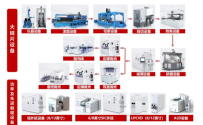
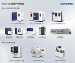
Maxsun's self-developed Micro LED MIP transfer stage solution integrates laser lift-off ( LLO ), laser mass transfer (LMT), laser cutting and other equipment, covering the entire process of Micro LED chips in the MIP process from epitaxial layer substrate peeling to mass transfer, precise cutting and separation. Among them, the laser mass transfer equipment used in the chip transfer link can achieve accurate and efficient transfer of hundreds of thousands or even millions of micron-level Micro LED grains, while also having an intelligent single chip replenishment function, which can significantly improve the production efficiency of the MIP process, reduce unit manufacturing costs, and effectively guarantee the yield, efficiency and quality of the client's Micro LED products.
The delivery of this solution also marks an important breakthrough for the company in the MIP packaging field, further increasing the market share of its Micro LED core process equipment.

Micro LED equipment advantages continue to consolidate
Relying on its profound accumulation in the field of laser technology, Maxsun Technology has independently developed Micro LED core process equipment and its supporting equipment, including laser lift-off, laser mass transfer, laser bonding, laser repair, laser decrystallineing, single-point bonding, substrate cleaning, small-particle cutting and other equipment, providing customers with high-efficiency, high-precision and high-stability mass production technology solutions.
Research on extreme ultraviolet radiation detection system and its calibration technology
Abstract
Objective
In-band energy is one of the key parameters of extreme ultraviolet (EUV) light sources. High in-band energy signifies higher photon flux and stronger exposure capability, while stable in-band energy ensures consistency and reliability in the lithography process. The detection of in-band energy enables the evaluation of EUV light source intensity and stability, providing essential guidance for system optimization and performance enhancement of EUV light sources. light source in-band energy measurements, precise calibration of the detection devices is required. Given that the spectral detection range of the device differs from the in-band spectral range, spectral calibration must be applied to the measured energy for accurate in-band energy calculation. In this study, we propose an EUV radiation detection system and analyze the impact of the key components characteristics on the system performance. Quantitative relationships between the component characteristics and in-band energy measurement accuracy are established, which leads to the optimization of the system structure. The system is calibrated using Hefei National Synchrotron Radiation Source. On this basis, the calculation method for the in-band energy of the EUV light source is optimized for the system, and an uncertainty analysis of the calculation results is conducted.
In-band energy detection is one of the core tasks for evaluating the performance of EUV light sources. In this study, an EUV radiation detection system is constructed for detecting the in-band energy of EUV light sources. The quantitative relationships between component characteristics and measurement precision are established by analyzing key parameters of the system, including the incidence angle, number of multilayer mirrors, reflective spectra of the mirrors, as well as the waveform broadening and response time of the detector. multilayer mirrors and a detector, is calibrated using the Hefei Synchrotron Radiation Source to determine its overall responsivity. Additionally, the transmittance of the filter is independently calibrated. On this basis, the calculation method for the EUV radiation detection system is optimized, resulting in a method to calculate the in-band energy of the light source from the narrowband energy detected by the system. Finally, the reliability of the EUV radiation detection system measurement results (at 13.5 nm) is quantified by evaluating five major sources of uncertainty, including the spectral responsivity of the EUV radiation detection system (excluding the filter), transmittance of the filter, oscilloscope integration signal, oscilloscope resistance, and solid angle.
Results and Discussions
Based on the analysis of multilayer mirror and the detector, an EUV radiation detection system is designed (Fig.7). For the radiation from the EUV light source, the size of the incident beam is limited by an aperture. The filtering is achieved using a Zr filter and two multilayer mirrors placed parallel with an incidence angle of 5°. The filtered radiation is received by the photodiode. After calibration, the transmittance curve of the Zr filter is multiplied with the system spectral responsivity curve, with the exception of the filter, to obtain the calibration result of the complete system. The calibration result is in good agreement with the theoretical curve (Fig.11). The spectral energy distribution obtained by the method of calculating the in-band energy of EUV light source is shown in Fig. 12, in which the in-band energy accounts for 59.78% of the total energy, and the calibration factor is 0.0284 A/W. The uncertainty analysis is presented in Table 2. The results indicate that the total uncertainty of the EUV radiation detection system measurements (at 13.5 nm) is 2.3%, which is mainly determined by the uncertainty of the system spectral responsivity except the filter (1.43%). By multiplying the total uncertainty by the t -value ( t =2.074), corresponding to the 95% confidence level, the expanded uncertainty of the system measurements (at 13.5 nm) is found to be 4.8%, which satisfies the industrial tolerance requirements for exposure dose measurement.
Conclusions
In this study, an EUV radiation detection system is designed and developed. The system utilizes a Zr filter and combination of two parallel-placed planar multilayer mirrors for spectral filtering. The system is calibrated using the Hefei National Synchrotron Radiation Source. On this basis, the calculation method of the EUV light source in-band energy is optimized for this system, and uncertainty analysis is conducted. Furthermore, the system is characterized in the wavelength range of 12.5 nm to 14.5 nm, with a central wavelength of 13.51 nm and a full width at half maximum (FWHM) of 0.43 nm. The spectral responsivity at the peak wavelength of 13.56 nm is 0.0150 A/W. The calibration factor for the calculation of the system EUV in-band radiation energy is 0.0284 A/W, and the expanded uncertainty at 13.5 nm is 4.8% ( t =2.074). This uncertainty level meets industry requirements, making the system suitable as a metrology tool for in-band energy detection of EUV light sources.
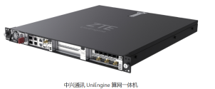
ZTE UniEngine computing and networking all-in-one machine successfully entered the first batch of product list of "5G+Industrial Internet" chain-building plan.
The 2025 Industrial Internet Conference was held in Suzhou, Jiangsu Province from May 21 to 23. As an important platform for accelerating the construction of new infrastructure, application exploration and practice, and industrial ecology of the Industrial Internet, and jointly exploring the path of deep empowerment of the industry, ZTE, as a leading company in the global ICT field, was invited to attend the conference.
During the conference, the first batch of product lists of the "5G+Industrial Internet" chain-building plan were officially released at the special event on collaborative innovation and development of new industrial networks and "5G+Industrial Internet". Ao Li, chief engineer of the China Academy of Information and Communications Technology, presented the certificate, and ZTE UniEngine computing and network all-in-one machine won the certificate.
ZTE UniEngine computing and network integration has passed the certification of China Academy of Information and Communications Technology Telecommunication Technology Laboratory, covering five dimensions: basic functions, ease of operation, reliability, security and industry adaptability. The UniEngine computing and network integration machine has passed the complete testing and certification, and the product information will be included in the "5G+Industrial Internet" chain-building plan directory to provide selection reference for industry customers.

ZTE UniEngine computing and networking machine has the following features:
1) Provide the industry's simplest 5G private network, integrating core network/wireless/network management, with features such as hourly rapid activation capability, network determinism, security isolation, and autonomous operation and maintenance, which greatly lowers the threshold for 5G industry private networks and meets the demands for intranet construction of industrial Internet enterprises.
2) Provide edge computing power, support virtual machine and container deployment, and APP lifecycle management to meet the enterprise's on-site application deployment requirements.
This product has been successfully deployed in dozens of industries including automotive manufacturing, electronic manufacturing, logistics, chemicals, steel, food, campuses, etc., helping the industry's digital transformation.


