Chinese semiconductor thread II

ansy1968

Brigadier
Registered Member
Another company supplying euv/duv/iline optics to SMEE, UEAscend and SiCarrier. There’s rumor UEA and SiCarrier took over SMEE’s advanced node DUV development team, so SMEE is now working on 28nm and older nodes only.

Please, Log in or Register to view URLs content!

Please, Log in or Register to view URLs content!
Thanks bro this is the news I'm been waiting, I had read it early this year BUT need to verify before posting. So Huawei will take the lead in developing both the EUV and DUV and if we are to believed THAT REPORT which I do, then Huawei had been using both the Improve SSA800A and the mythical SSA900A in their production line, mind you the performance level of the former and the latter is akin to ASML NXT2000i and NXT2050i. It might be a stretch BUT I'm leaning more to what @sunnymaxi had posted about Huawei producing its own 5nm chip, whether in collaboration with SMIC or not its seems like they have the capability to do so.

What interest me the most is the SMIC Beijing FAB, one of the 4 major FAB expansion of SMIC together with Shanghai Lin-gang, Tianjin and Shenzhen. From the grapevine it will be using all domestic tool with 7nm line being established.
 

european_guy

Junior Member
Registered Member
Another company supplying euv/duv/iline optics to SMEE, UEAscend and SiCarrier. There’s rumor UEA and SiCarrier took over SMEE’s advanced node DUV development team, so SMEE is now working on 28nm and older nodes only.

Please, Log in or Register to view URLs content!

Please, Log in or Register to view URLs content!

While reading about the above
Please, Log in or Register to view URLs content!
, I stumbled on these guys:

Please, Log in or Register to view URLs content!


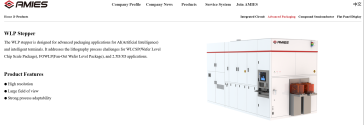
1748327702827.png


They are from Shanghai (like SMEE) and they do lithography for advanced packaging (like SMEE)

What really got me is
Please, Log in or Register to view URLs content!
:

Shanghai AMIES Technology Co., Ltd. (English name: AMIES Technology Co., Ltd. ) was established in February 2025.

The company's technical team has about 600 peoplewith an average age of 33, and 65% have master's and doctoral degrees.

Established 3 months ago? Now already 600 people in R&D and a full product line?

Who are they? Did SMEE business units split?

BTW even their logo is similar to SMEE's one....
 

tokenanalyst

Brigadier
Registered Member
While reading about the above
Please, Log in or Register to view URLs content!
, I stumbled on these guys:

Please, Log in or Register to view URLs content!


View attachment 152967


They are from Shanghai (like SMEE) and they do lithography for advanced packaging (like SMEE)

What really got me is
Please, Log in or Register to view URLs content!
:


Established 3 months ago? Now already 600 people in R&D and a full product line?

Who are they? Did SMEE business units split?

BTW even their logo is similar to SMEE's one....
Could be the SMEE getting rid of the packaging division to get into frontend litho more seriously.
 

tokenanalyst

Brigadier
Registered Member

Zhuhai breaks through the semiconductor equipment industry, and the first wafer-level multi-drive dissociation and etching equipment in China is launched​

Zhuhai, Guangdong, is one of the earliest cities in China to start integrated circuits, but the design industry has long been the dominant industry . Now, the city is moving into the relatively weak manufacturing sector.

Recently , Zhuhai Hengge Microelectronics Equipment Co., Ltd. released the country's first wafer-level plasma multi-drive dissociation etching equipment, marking a major technological breakthrough in the field of core equipment for domestic high-end semiconductor manufacturing.

The equipment has broken through many " bottleneck " technical difficulties and has the characteristics of high efficiency, high uniformity and high compatibility. It can be widely used in integrated circuits, third-generation semiconductors and advanced packaging fields, and is suitable for 8- inch to 12- inch wafer manufacturing needs.

Hengge Microelectronics told Jiemian News that it has reached cooperation with two companies, one of which is a leading domestic display panel company. The two parties have reached a process cooperation and development agreement. They will carry out joint research and development for the etching process needs in display panel manufacturing, and promote the large-scale application of domestic plasma etching equipment in the display field.

1748356278809.png

Please, Log in or Register to view URLs content!
 

tokenanalyst

Brigadier
Registered Member

Huaxin Micro-Nano's "8-inch MEMS wafer fully automatic production line" officially put into production​


According to Bengbu News, on May 24, Anhui Huaxin Micro-Nano Integrated Circuit Co., Ltd. announced that the first batch of products from its 8-inch wafer production line had been successfully put into production, marking the official start of production of the country's first 8-inch MEMS wafer fully automatic production line in Bengbu.
1459001260846.8147.jpg

It is understood that Huaxin Micro-Nano is mainly engaged in MEMS wafer manufacturing, and its processable products include inertial sensors, pressure sensors, optical MEMS devices, etc., which are mainly used in high-end equipment, automotive electronics and other fields. This project is the country's first 8-inch MEMS wafer fully automatic production line and the country's first piezoelectric MEMS mass production line with complete process equipment. After it is fully completed and put into production, it will have the capacity to produce 30,000 wafers per month, becoming the largest MEMS wafer production line in China.

Recently, Ding Jingxiu, deputy general manager of Huaxin Micronano, introduced that "the company has reached cooperation intentions with 50 customers, signed a total of 210,000 wafers, and signed contracts worth 120 million yuan. Another 30,000 wafer contracts are under negotiation, which will effectively support the production of 10,000 wafers in 2025. There are currently 13 serial products, 6 of which have completed the full process engineering batch tape-out and started debugging and production. It is planned to be delivered to customers for function and reliability verification before the end of June."

Please, Log in or Register to view URLs content!
 

tokenanalyst

Brigadier
Registered Member

This ceramic company will accelerate the localization process of silicon nitride ceramic substrates​


Fanyi Fine Ceramics has completed a financing of tens of millions of yuan to accelerate the localization process of silicon nitride ceramic substrates and silicon carbide semiconductor components. Recently, Zhongxing Capital announced that it has completed the lead investment of tens of millions of yuan in the A round of financing for Lanxi Fanyi Fine Ceramics Co., Ltd. (hereinafter referred to as "Fanyi Fine Ceramics"), and joined forces with a number of industrial parties to increase investment in the field of new materials. Zhongxing Capital and Fanyi Fine Ceramics have joined hands to accelerate the localization process of silicon nitride ceramic substrates and silicon carbide semiconductor components, and promote the independent control of key materials.

Fanyi Fine Ceramics has a production base of over 30,000m2, specializing in the research and development and production of structural ceramics and functional ceramic materials, as well as providing customers with customized ceramic material solutions. The company has a variety of processes such as micro-nano powder preparation, ceramic molding, cold isostatic pressing, atmospheric pressure sintering, hot pressing sintering, reaction sintering precision ceramic machining, etc. The main products include neutron absorbing boron carbide ceramics, neutron absorbing balls, boron carbide ceramics, silicon carbide ceramics, boron nitride composite ceramics, silicon nitride ceramics, etc. Many new products have filled the domestic gaps and reached the international advanced level. The company produces various ceramic products that are widely used in China's nuclear industry, equipment, aerospace, semiconductors, metallurgy, electronics and other fields.​


Please, Log in or Register to view URLs content!
 

tokenanalyst

Brigadier
Registered Member

Experimental Study on Characteristics of Isopropanol Ejection Driven by Electrohydrodynamics.​

Abstract​

A droplet generator is one of a key module for realizing the Sn-LPP EUV light source. One way of improving a conversion efficiency (CE) and relax tin contamination issue of Sn-LPP EUV light source is to produce tin droplet targets with suitable size. Less than several 10-um nozzles are used to generate tin droplets. Particles from environment and chemical reaction compounds with high temperature tin cause nozzle clogging issue often. It is significant to develop a technical approach using a large diameter nozzle to produce mass-limited targets. Therefore, this paper demonstrated droplet ejection experiments based on Electrohydrodynamics (EHD). Characteristics of isopropanol (IPA) droplet ejection by EHD droplet production platform that was designed and constructed in our laboratory. Characteristics of various process parameters on the IPA droplet production process were investigated. Images of droplet formation process were observed with using a droplet observation system and analyzed by image analysis software. Consequently, the smallest IPA droplet with a diameter of 13 μm could be produced using a nozzle with a diameter of 50 μm. Additionally, EHD method could make droplets from 13 μm to 55 μm with applying voltage from 5.5 kV to 2.5 kV. In the future, EHD will apply to make mass-limited tin droplet targets under vacuum and high-temperature conditions, in order to increase the CE and to decrease tin debris.

Please, Log in or Register to view URLs content!
 

tokenanalyst

Brigadier
Registered Member

Leading manufacturer receives another order for silicon carbide equipment.​


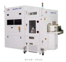
ZhongdaoOptoelectronics disclosed that the company's NanoPro-150 nanometer-level wafer inspection equipment has once again received a repeat order from a leading customer in the global silicon carbide (SiC) industry, and will be used for defect detection in the front-end process of the customer's 8-inch SiC wafers.

Compared with traditional 6-inch SiC wafers, 8-inch SiC has significant advantages in unit cost, production efficiency and yield control, and is the mainstream direction of the future power semiconductor industry. The chairman of Zhongdao Optoelectronics said that the localization rate of the company's NanoPro-150 series equipment has reached more than 95%, which greatly reduces the equipment investment cost of customers while ensuring performance.
1748361354106.png


This order is the second additional order from the customer within half a year, following the bulk purchase at the beginning of this year. The order was obtained after three months of rigorous technical benchmarking, and NanoPro-150 fully met the core indicators such as detection efficiency, stability and data traceability.

Earlier in January, Zhongdao Optoelectronics stated that it plans to invest more R&D resources in the field of nano-level defect detection of SiC wafers, and further improve the quality and efficiency of SiC wafer manufacturing through the upgrade of high-precision multi-mode defect detection technology, system optimization of artificial intelligence (AI) defect recognition algorithms, and improvement of overall equipment performance.

Currently, the company is developing the next generation of inspection equipment, NanoPro-200 and NanoPro-300, which will have higher inspection accuracy and wider process coverage. Among them, the technical specifications of NanoPro-200 have reached 40 nanometers, and it has made significant breakthroughs in AI intelligence and automation. The third generation NanoPro-300 has also entered the critical period of research and development.

Please, Log in or Register to view URLs content!
 
Top