Chinese semiconductor thread II

tokenanalyst

Brigadier
Registered Member

Dinglong: Strive to be the support and leader of material innovation in the semiconductor display industry​


In 2023, Dinglong Technology, with its amazing determination and innovative spirit, led the domestic OLED display industry to achieve an epoch-making milestone: achieving the industrialization goal of PSPI photoresist annual production capacity reaching 1,000 tons. Today, Dinglong (Xiantao) Semiconductor Materials Industrial Park has not only stably produced multiple batches of PSPI photoresist products for OLED displays, but also successfully transported them to downstream clients, further ensuring China's new display industry supply chain Safety , and the original intention of technological innovation and independent supply, have promoted the vigorous development of the domestic new display industry.

Looking back ten years, Dinglong Co., Ltd. drew inspiration from the "three primary colors of pigments" of its traditional main product - color polymeric toner, and successfully transformed into the new field of "displaying three primary colors" of OLED. In 2017, Dinglong Co., Ltd. used its independent subsidiary Flexible Display Technology as a platform to focus on the flexible display materials business and officially entered the materials branch of OLED's third-generation mainstream display technology. At the same time, the company has also forward-lookingly laid out key "stuck neck" materials in the LCD, Micro-LED display fields and advanced packaging, demonstrating its profound market insight and technical strength.

This year is the seventh year that Dinglong has entered the semiconductor display materials industry. In order to maintain the continued competitiveness of its products and keep up with the speed of technological iterations of downstream customers, the company follows the main line of PI high-performance materials and continuously expands and develops products including polyimide (YPI), photosensitive polyimide (PSPI) ), black photoresist (BPDL), PI alignment liquid, thin film encapsulation ink (TFE INK), encapsulation photoresist, etc., more than 30 "stuck neck" material products. As a result, Dinglong has become the only innovative material platform company in the field of domestic semiconductor display materials that can compete with more than a dozen international giants at the same time, providing customers with a full range of innovative material products and technical service solutions.

Please, Log in or Register to view URLs content!
 

tokenanalyst

Brigadier
Registered Member
Accurate assessment or just cope?

“It is too early to identify the potential influence China would have on the HBM market. But we are skeptical about CXMT succeeding in developing the delicate technology required to produce HBM,” an industry official said under the condition of anonymity.

“CXMT has been saying it will master the production of advanced DRAM chips for the past decade, but it still struggles with conventional DRAMs. I believe it would be difficult for China to catch up to the HBM technology of current players in 4-5 years.”


Please, Log in or Register to view URLs content!

The rule of thumb if everytime a stooge says that will take China X amount of time to achieve something I always subtract years or even a entire decade depending on the tech in question, the urgency that Chinese companies and institutions have for the technology in question, how accessible is from outside and how much of the tech in question is already developed in China.

And even if that was "accurate", like 4 years, we should remember that the pandemic was 4 years ago and time just passed. Another thing is people said it like if China will just start the development HBM tech after 4 years but in reality China in 2 years could have mastered like 80% of the technology and already start the commercialization.
 

gotodistance

New Member
Registered Member
Accurate assessment or just cope?

“It is too early to identify the potential influence China would have on the HBM market. But we are skeptical about CXMT succeeding in developing the delicate technology required to produce HBM,” an industry official said under the condition of anonymity.

“CXMT has been saying it will master the production of advanced DRAM chips for the past decade, but it still struggles with conventional DRAMs. I believe it would be difficult for China to catch up to the HBM technology of current players in 4-5 years.”


Please, Log in or Register to view URLs content!

Korea's trash media is overflowing with fake news that even Koreans don't see. In the last two years, fake news has been making news in the Korean media, and there are too many stupid Koreans who believe it. You don't have to care about Korean news. Fake news with no experts or connections in China
 

tokenanalyst

Brigadier
Registered Member

Jintuo Co., Ltd.: The semiconductor special equipment business has achieved key breakthroughs based on core technologies in the thermal field and has provided products and services to approximately 48 customers.​


The company replied: The company's semiconductor special equipment business has achieved key breakthroughs based on core technologies in the thermal field. Currently, it has developed and produced a number of domestic blank semiconductor thermal equipment with certain technical barriers, which can be applied to a variety of advanced packaging processes. It provides products and services to large-scale packaging and testing manufacturers at home and abroad, and has the ability to customize different manufacturing process equipment for customers. The company's semiconductor special equipment products have been delivered to and served by approximately 48 customers so far, including typical downstream core packaging and testing manufacturer customers, and have been recognized, accepted and repurchased by customers.

1715102038320.png
Please, Log in or Register to view URLs content!
 

tokenanalyst

Brigadier
Registered Member

The largest SiC power semiconductor manufacturing base in China ushered in a new node​

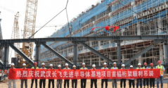
Wuhan YOFC Advanced Semiconductor Base Project successfully completed the hoisting of the first truss, marking the full launch of the steel structure construction of the project.

1715105424511.png
Recently, the Wuhan YOFC Advanced Semiconductor Base project, the largest SIC power semiconductor manufacturing base in China undertaken by China Construction First Engineering Bureau Construction and Development Company, successfully completed the hoisting of the first truss, marking the full start of the steel structure construction of the project and helping Wuhan build a world-class compound Semiconductor industry highland.

The project is located in Wuhan City, Hubei Province, with a total construction area of approximately 251,500 square meters. After completion, it is expected to produce 360,000 6-inch silicon carbide MOSFETs and wafers annually, and 61 million power device modules. It will widely cover new energy vehicles, photovoltaics, and storage. energy, charging piles, power grids and other fields.

Please, Log in or Register to view URLs content!
 

tokenanalyst

Brigadier
Registered Member

With a total investment of US$100 million, Liyan Semiconductor Project was signed in Changzhou, Jiangsu​


On April 29, the Liyan Semiconductor Changzhou Industrial Base launch and semiconductor fund signing ceremony was held.

It is understood that this project is a major project in Jiangsu Province in 2024, with a total planned investment of US$100 million, a total land area of 75 acres, and new production plants, comprehensive buildings, semiconductor industry research institutes and ancillary buildings. It is planned to be completed and delivered in 2025. The project After reaching production, it will achieve annual sales revenue of 1 billion yuan. It is reported that the target products of this project are advanced semiconductor manufacturing processes and precision testing equipment. After the project is completed, it will form a production scale of 360 units per year, including 120 units of wafer cleaning and polishing equipment, 120 units of wafer thinning and grinding equipment, and wafer inspection equipment. 120 pieces of equipment.

Please, Log in or Register to view URLs content!
 

Wrought

Junior Member
Registered Member
Looks like Intel and Qualcomm are no longer allowed to sell some components to Huawei (not clear exactly which). Apparently this was driven by Congressional handwringing. Can't see it having much of an impact given the current trend towards domestic suppliers. Speaking of, was there ever a clear answer for P70?

Marco Rubio, the Republican vice-chair of the Senate intelligence committee, and Elise Stefanik, the fourth-ranking Republican in the House of Representatives, last month urged Raimondo to revoke Huawei licenses after reports emerged that the Shenzhen-based group had built laptops using chips from Intel.

“It is clear from these trends that Huawei, a blacklisted company that was on the ropes just a few years ago, is making a comeback,” the lawmakers wrote in their letter.
Please, Log in or Register to view URLs content!

It must really grind their gears to Huawei thriving.
 

tokenanalyst

Brigadier
Registered Member

The Natural Science Foundation of China released the 2024 Project Guidelines for the Scientific Basics Major Research Plan on Frontier Technology of Integrated Chips, with a maximum of 15 million yuan per project.​


2. Core scientific issues

This major research plan focuses on the problems of decomposition, combination and integration of integrated chips after the number and types of core particles have been greatly increased, and focuses on the following three core scientific issues:

(1) Mathematical description and combinatorial optimization theory of core particles.

Explore the abstract mathematical description method of integrated chips and core particles, and construct the mapping, simulation and optimization theory of complex functions from integrated chips to core particles.

(2) Large-scale chip parallel architecture and design automation.

Explore the integrated chip design methodology after the chip integration level has been greatly improved, study multi-core interconnection architecture and circuits, layout and routing methods, etc., to support the design of hundred-core/ten thousand-core scale integrated chips.

(3) Multi-physics coupling mechanism and interface theory at the core particle scale.

Clarify the mutual coupling mechanism of electric-thermal-force multi-physics in integrated chips under the three-dimensional structure, build a fast and accurate simulation calculation method for multi-physics and multi-interface coupling at the core particle scale, and support the design and manufacturing of 3D integrated chips.


(1) Cultivation projects.

Based on the above scientific issues and driven by the overall scientific goals, in 2024, it is planned to give priority to funding application projects that are exploratory, have original ideas, and propose new technological paths around the following research directions:

1. Core particle decomposition and reusable design method.

Research the formal description of integrated chips and core particles, decomposition-combination theory and modeling methods, and study reusable design methods of core particles such as computing/storage/interconnection/power/sensing/radio frequency.

2. Multi-core parallel processing and interconnection architecture.

Research on high computing power and scalable architecture for 2.5D/3D integration, interconnection networks and fault-tolerance mechanisms between cores such as computing/storage/communication, multi-core heterogeneous compilation tool chains, etc.

3. Integrated chip multi-field simulation and EDA.

Research on electro-thermal-mechanical coupling multi-physics calculation methods and rapid simulation tools for the core particle scale, integrated/layout/wiring automated design tools for integrated chips, testability design of integrated chips, etc.

4. Integrated chip circuit design technology.

Research on high-speed, energy-efficient serial/parallel, radio frequency/wireless, silicon optical interface circuits for 2.5D/3D integration, power management circuits and systems for high-power integrated chips, etc.

5. Integrated chip 2.5D/3D process technology.

Research the manufacturing technology of large-size silicon substrates (Interposer), high-density and highly reliable 2.5D/3D integration processes and materials, heat dissipation methods for 10,000-watt chips, optoelectronic integrated packaging processes, etc.

(2) Key support projects.

Based on the core scientific issues of this major research plan and driven by the overall scientific goal, in 2024, it is planned to give priority to funding application projects with good accumulation of early research results, strong cross-cutting, and greater contributions to the overall scientific goal:

1. Cache coherence and storage systems.

Study the cache coherence mechanism of heterogeneous multi-core systems, explore the multi-level cache architecture of integrated chips, scalable storage management mechanisms, and on-chip network-based memory access optimization strategies and quality of service (QoS) optimization mechanisms. Construct a behavior-level model of cache consistency between cores, supporting cache consistency between ≥ 2 types of heterogeneous cores (CPU, GPU, etc.), the total number of CPU cores ≥ 256, and the stable state of ≥ 7 cache lines. Typical latency is <200 cycles, and an open source functional verification simulator is available.

2. Core particle decomposition and combination optimization method.

For computing scenarios such as end-edge-cloud, study core particle decomposition and combination optimization theory, explore the functional representation of core particles, establish mapping of complex applications to core particles, study the stability and robustness of mapping theory, and form a complete Core particle library construction method.

3. Layout and wiring method of multi-reticle integrated chip.

With the goal of minimizing the number of mask layers and cross-mask interconnections in silicon substrate manufacturing, study the automated layout and wiring method of multi-mask integrated chips, and explore the TSV/interconnect line/deep trench capacitor process and design collaborative optimization method.

4. Testability design method for integrated chips.

Research the integrated chip test bus architecture with high testability, plug-and-play and low overhead, break through the bottleneck caused by limited observable pins, explore hierarchical test scheduling and fault diagnosis technologies for integrated chips, and achieve testability Design EDA tools and open source them, with interconnection fault coverage ≥99% and test architecture hardware overhead ≤5%.

5. Energy-efficient chip-to-chip interconnect single-ended parallel interface circuit.

Research high-energy-efficiency, high-density 2.5D parallel interconnect interface circuit technology.

6. Multi-field simulation algorithm and solver for core particle scale .

Research the electro-thermal-mechanical coupling model for the core particle integration process, explore the multi-physics simulation numerical method of the key structure, materials and interfaces of the integrated chip, realize automatic calculation grid division, develop a cross-scale multi-field simulation solver and Open source, the error range of calculation accuracy and experimental results is less than 10%.

7. Large-size silicon substrate manufacturing technology and warpage model and stress optimization.

Research large-size silicon substrate (Interposer) manufacturing technology, build wafer-level warpage models and stress optimization methods, and explore the stress of high-density, high-aspect-ratio through-silicon vias (TSV), deep trench capacitors (DTC) and other manufacturing processes .

8. Three-dimensional integration of efficient heat dissipation materials and structures.

Explore the heat distribution characteristics and efficient heat transport mechanism under strong coupling of multiple hot spots, the integration of new heterogeneous heat dissipation materials and interface heat transport control methods, the structural design of micro-channel radiators and enhanced heat transfer methods.

(3) Integration projects.

This year, it is planned to select research directions with significant application value and good research foundation for integrated funding. The specific research directions are as follows:

1. Heterogeneous computing three-dimensional integrated chip.

Research cross-level collaborative design methods for three-dimensional integrated chips, explore modular combination and optimization methods of heterogeneous cores, and verify key technologies such as vertical power supply architecture and circuits, automated silicon substrate layout and wiring, and high-density core-wafer bonding.

Please, Log in or Register to view URLs content!
 

tphuang

Lieutenant General
Staff member
Super Moderator
VIP Professional
Registered Member
bringing this back up in light of my other research about abundance of sub 3GHz RF filter, but not enough higher frequency n78/n79 filters.

Please, Log in or Register to view URLs content!

so they have their own n79 BAW filters. size just 1.4mm x 1.1mm, so you can make a lot of them per wafer (65-70k per wafer based on my calculation. using 70% yield, you can get 45-50k/wafer) -> matches what Sai Micro said about BAW filter it produces for memsonic

120k wpy x 50k chip/wafer = 6B chip/year if this get ramped up. If 3GHz and above represent 1/3 RF filter (let's say 30), then this is enough for 200m 5G phones

but in this case, just like in memsonic, it's going to take a while for production to be ramped up

Please, Log in or Register to view URLs content!

Presently, just 20m deliveries/month, so adding this new production line will increase capacity by a lot. But I would imagine even the production line they have now is likely to have a lot more capacity to ramp up

Please, Log in or Register to view URLs content!

more on these guys

Their production line for 10k wpm of 5G filters have seen its new factory roofed. This facility required 750m RMB in investment. Maybe it will go into production this year of the n79F filters
 

gelgoog

Lieutenant General
Registered Member
Accurate assessment or just cope?

“It is too early to identify the potential influence China would have on the HBM market. But we are skeptical about CXMT succeeding in developing the delicate technology required to produce HBM,” an industry official said under the condition of anonymity.

“CXMT has been saying it will master the production of advanced DRAM chips for the past decade, but it still struggles with conventional DRAMs. I believe it would be difficult for China to catch up to the HBM technology of current players in 4-5 years.”
The main question is who would CXMT sell this memory to. SK Hynix had a deal with AMD. Would, say, Huawei buy this HBM for their AI Ascend chips or something? Would sales be enough to justify developing HBM?

It is just DRAM. With TSVs and micro bump connections. YMTC already uses TSVs in its VNAND, and Huawei HiSilicon uses micro bumps in the packaging for the Kirin 9010. Talk that the basic technology is not used in China is just plain bullshit.

Looks like Intel and Qualcomm are no longer allowed to sell some components to Huawei (not clear exactly which). Apparently this was driven by Congressional handwringing. Can't see it having much of an impact given the current trend towards domestic suppliers. Speaking of, was there ever a clear answer for P70?
Talk about closing the barn door after the horse bolted away. Now that Huawei has the SMIC manufactured Kirin 9010 with the latest Taishan cores they do not need more Qualcomm chips. Just look at their smartphone lineup. Only the low end phones still might use Qualcomm chips. And those are just legacy phones which they have not replaced yet. As for Intel the Taishan core is powerful enough to make an analogous chip to the Apple M1 to put in a laptop. Remove the 5G modem and put more CPU and GPU cores. These people are really dumb.
 
Top