Chinese semiconductor thread II

tokenanalyst

Brigadier
Registered Member

Zhongke Feichai: New products of inspection and measurement equipment continue to expand equity incentives, demonstrating confidence in long-term revenue growth​


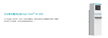
New product revenue continues to increase, and we are actively developing 2Xnm nano-pattern wafer defect detection equipment. In the front-end field, the company's revenue mainly comes from non-patterned and (micron-level) patterned wafer defect inspection equipment and three-dimensional topography measurement equipment. New growth points include photolithography overlay accuracy measurement equipment and metal/dielectric film thickness measurement. equipment, and actively develop nano-pattern wafer defect detection equipment. Among them.

1-overlay accuracy measurement equipment has been supplied in batches at mature process nodes, and has been verified by some customers in advanced process production lines;

2-multiple metal film thickness measurement equipment has been shipped in batches;

3-for the 2Xnm node, the company clearly stated The research and development of dark field nanopattern wafer defect detection equipment and critical dimension measurement equipment are progressing smoothly;

4-For the 1Xnm node, the company has continued to develop and deploy a variety of detection and measurement equipment.

The company's advanced packaging equipment lays out graphics wafer defect detection and three-dimensional topography measurement equipment, and its growth trend is improving. The most important inspection and measurement equipment used in the field of advanced packaging include pattern wafer defect inspection equipment, critical dimension measurement equipment, wafer dielectric film measurement equipment, and three-dimensional topography measurement equipment. The company's advanced packaging machines include.

1-graphic wafer defect detection equipment, which can be used for sub-micron two-dimensional and three-dimensional inspection of wafer surfaces. Customers include Changdian Advanced Technology, etc.;

2-three-dimensional topography measurement equipment, which is used for nano-level three-dimensional topography. Measurement, double/multi-layer film thickness measurement, critical dimensions and offset measurement, customers include Changdian Advanced, Changdian Shaoxing, etc. Considering that overseas HBM and other companies have recently generated demand for advanced packaging, and corresponding inspection and measurement equipment leaders such as Camtek and others have indicated strong demand, the growth trend of Zhongke Feichi's advanced packaging equipment is also expected to be positive.

Please, Log in or Register to view URLs content!
 

tphuang

Lieutenant General
Staff member
Super Moderator
VIP Professional
Registered Member

Ruishi Technology launches two-dimensional addressable VCSEL chips for lidar and obtains mass production orders ..​


With the rapid development of automobile intelligence and autonomous driving technology, the automotive lidar (LiDAR) market has shown rapid growth in recent years. According to Mams Consulting, Ruishi Technology recently launched a new two-dimensional addressable lidar VCSEL chip, which can be applied to smart driving solutions equipped with solid-state lidar to achieve higher-level smart driving functions. At present, this new product has received mass production orders from major lidar manufacturers, and Ruishi Technology has become the first manufacturer in the industry to mass produce two-dimensional addressable VCSEL products.

Two-dimensional addressable VCSEL drives solid-state lidar solutions

As an ideal light source for pure solid-state lidar, two-dimensional addressable VCSEL can achieve the effect of zoned lighting, so that the whole machine does not contain any moving parts, which greatly improves the reliability of lidar and provides solutions for lidar applications. More possibilities. Compared with one-dimensional addressing, two-dimensional addressing requires major adjustments to the epitaxial design, chip process, chip testing and other aspects of the VCSEL chip, and the complexity of the driving scheme is also greatly increased, which has a comprehensive impact on VCSEL manufacturers. Ability is a great test.

Ruishi Technology's two-dimensional addressable area array VCSEL technology supports flexible scanning modes, which can greatly improve energy utilization. Compared with one-dimensional scanning, its power consumption and heat dissipation are more friendly, and it can be dynamically adjusted in real time according to different ranging scenarios. Local transmit power to achieve the optimal energy ratio.

The first 100% domestic supply chain in China

As one of the few manufacturers in the world that can provide two-dimensional addressable VCSEL, Ruishi Technology's two-dimensional addressable VCSEL not only has high-precision and high-reliability sensing capabilities, but also achieved a nationwide supply chain for the first time in the industry. This not only means that Ruishi Technology has achieved independent control in all aspects of chip R&D and production, improving the stability of chip supply, but also greatly reducing chip production and packaging costs.

Please, Log in or Register to view URLs content!

@tphuang ..


This is actually just showing how much VCSEL tech has been industrialized. You can see that they are even putting it in smart vacuum cleaners now. Just absolutely crazy how cheap these things are getting
 

AssassinsMace

Lieutenant General
They can always sell to US military customers as well as US government that need these 5nm chips. But how many do they need is a huge question.

I think the volume is pretty small compare to the commercial market.

Also depending a lot on the state of the US encomny, if there is a major recession like 2009. Then it is game over for that fab. :eek:
Yes the commercial market at its fullest is always more profitable. China alone before the US’s chip ban was 60% of world’s semiconductors business, larger than all the West combined.

When China develops equivalent to better chips than the West, their semiconductor business will eventually die. Yeah sure they can force their own companies to buy their own more expensive chips but in the commercial market cheaper always wins or else whatever commercial business that needs them goes bankrupt because there will be international competitors that will be using cheaper Chinese semiconductors. Not to forget also that in Western stock markets making the most money possible is paramount to a company’s stock value. More expensive chips means less profits.
 

Randomuser

Senior Member
Registered Member
NAURA
AMEC
SMEE
Piotech

These are the semiconductor equipment companies in China to look out for since they will be key to winning the war.

Are there any other players that will become important in the future?
 
Top