Chinese semiconductor thread II

european_guy

Junior Member
Registered Member
Whatever decision, the trust is broken already

I understand Nexperia CEO was suspended by a Dutch court. Formally this means only the court could reinstate him...but IMHO is very unlikely that judges will revert their decisions (they are not politicians).

It could be found a compromise with the Ducth government without changing the court decision, like agree on a new Chinese CEO, but this is not the core of the issue.

The real issue is what to do with Nexperia in the future. IMHO the most natural outcome is that the European branch is sold and the current Chinese owner keep the Chinese branch including assets and IP, and maybe also the brand rights for a reasonable period. In the medium/long term Western customers will remain with Nexperia only if is under western control...and probably the opposite is true for Chinese customers.

But the real outcome could be an accelerated decoupling from Chinese chips by Western customers.

I understand why China played their cards in that way, but when you chose one road, for whatever good reason, you have to be ready to live with the consequences of your choice. See US with semi in China, this is the posterchild of short term decisions that have long term (opposite) consequences. Now China will reach technological independence, no matter what.

I'm not criticizing China, they had all the rights to do what they did...but in international geopolitics, acknowledge of who is right, this has no value. What it counts are the consequences of your actions in the long term. Here I see an acceleration toward long term decoupling of chips, after the chip machinery/tools that are already well within decoupling phase.
 

tphuang

General
Staff member
Super Moderator
VIP Professional
Registered Member
Alright, let's keep this off your opinion of the Nexperia matter and just get back to posting actual news releases on it.
 

tphuang

General
Staff member
Super Moderator
VIP Professional
Registered Member
Please, Log in or Register to view URLs content!

陕西光电子先导院总经理杨军红介绍陕西“追光计划”阶段性进展,宣布光电子先导院建设的“8英寸先进硅光集成技术创新平台”(简称“8英寸硅光平台”)已正式通线,并发布了一款无源SOI(绝缘衬底上的硅)集成超低损耗氮化硅产品的PDK(工艺设计套件)。
陕西光电子先导院 has introduced 8-inch advanced Silicon Photonics production line and released a PDK for passive SOI integrated ultralow loss Silicon Nitride product. This will allow them to work on process above 90nm. Customers are SiPO & optoelectronic customers
 

tokenanalyst

Lieutenant General
Registered Member

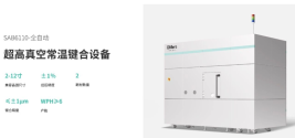
Qinghe Epistar's room-temperature bonding equipment has been recognized by an overseas semiconductor customer and successfully implemented in its production line.​


Qinghe Epistar's independently developed SAB61 series product, the "Fully Automatic Ultra-High Vacuum Room Temperature Bonding Equipment," successfully completed the customer's pre-acceptance test and was officially delivered to an overseas semiconductor customer and installed on their production line.
1762265191446.png
The production line delivered this time has extremely high requirements for equipment stability, precision, and process consistency, which signifies that the company's [ultra-high vacuum room temperature bonding equipment] has gained recognition from the international high-end market for its comprehensive performance.
1762265171258.png

Ultra-high vacuum room-temperature bonding equipment utilizes ultra-high vacuum ion beam bombardment technology to activate material surfaces, achieving strong covalent bonds without heating or annealing. It boasts high bond strength, supports bonding of heterogeneous materials (such as SiC, Ga₂O₃, and diamond), and eliminates thermal stress and interface oxide layers. Applications encompass composite substrates, MEMS, heterogeneous integration with high heat dissipation requirements, multi-segment solar cells, optical crystal integration, and flexible electronics.

Please, Log in or Register to view URLs content!
 

tokenanalyst

Lieutenant General
Registered Member

Luwei Optoelectronics: Mass production of 180nm process node semiconductor photomasks has been achieved​

Luwei Optoelectronics stated on its interactive platform that it has achieved mass production of 180nm process node semiconductor photomasks, and its 150nm/130nm processes have passed customer verification and entered small-batch mass production. The Luwei Semiconductor project, invested and constructed by the company, is positioned for 130-28nm photomask manufacturing, placing it among the leading domestic manufacturers in process node layout. Currently, samples of 90nm and above semiconductor photomasks have been sent to customers and have passed verification by some. Trial production of 40nm semiconductor photomasks will begin in the second half of 2025, and the project is progressing smoothly.

According to public information, Luwei Optoelectronics is a company specializing in photolithography masks. Founded in 2012, it has two core product lines: flat panel display masks and semiconductor masks. It is the only domestic manufacturer with the capability to produce masks across all generations, from G2.5 to G11. In the third quarter of 2025, Luwei Optoelectronics achieved operating revenue of 827 million yuan, of which quartz masks accounted for 499 million yuan (91.80%) and soda ash masks accounted for 41.3049 million yuan.

Please, Log in or Register to view URLs content!
 

tokenanalyst

Lieutenant General
Registered Member
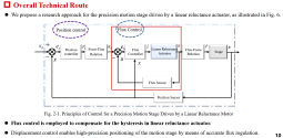
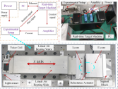
Harbin developing the actuators for the next generation of lithography wafers scanners.
1762266009529.png

A compensation method for electromagnetic hysteresis: Application in linear reluctance actuator​

Abstract​

The linear reluctance actuator is a specialized electromagnetic actuator that generates motion based on the reluctance effect. With its high force density and lower power consumption, it presents advantages over Lorentz actuators, which are commonly used in lithography machines. This actuator has the potential to overcome the physical limitations of voice coil motors, which struggle to achieve the high acceleration required for next-generation lithography systems. The complex hysteresis nonlinearity between current and magnetic flux density in linear reluctance actuator, stemming from electromagnetic hysteresis, eddy currents, and motion coupling, induces force deviations that limit their broader application. In this paper, we present a hysteresis model that relates current and flux, developed using flux measurements from sense coils. By integrating this model with the adaptive feedforward parameter tuning method, hysteresis nonlinearity is effectively compensated, enabling precise flux control. Experimental results demonstrate that the model effectively captures the actuator’s rate-dependent hysteresis behavior, and the proposed method effectively compensates for hysteresis nonlinearity.​
1762266106228.png

1762265973482.png

Please, Log in or Register to view URLs content!
 
Top