Chinese semiconductor industry

Status
Not open for further replies.

gelgoog

Lieutenant General
Registered Member
AFAIK the initial 28nm immersion lithography tools by SMEE are not optimized for multiple patterning of the kind used in 14nm or smaller.
They are supposed to introduce a model a year or two afterwards that is optimized for that.

But then again SMIC is not using the latest and greatest ASML DUV to produce their 14nm chips either.

BTW here are some old quotes of comments by the ASML CEO on the whole situation.

Please, Log in or Register to view URLs content!

"Export controls against China will not only fail to halt its technological progress but also hurt the U.S. economy, ASML Holding NV Chief Executive Officer Peter Wennink said, after trade tensions between Washington and Beijing led to restrictions on the sale of the Dutch company’s advanced chip equipment to Chinese firms.

I believe that export controls are not the right way to manage your economic risks if you have determined that there is an economic risk,” Wennink said during an online industry event on Wednesday, arguing that if “you close China from access to technology, that will also cost non-Chinese economies a lot of jobs and a lot of income.”"


Please, Log in or Register to view URLs content!

"China's move toward self-sufficiency in semiconductors raises new questions on the future of existing global players. Peter Wennink, CEO of ASML, a leading manufacturer of lithography equipment for the production of computer chips, recently told news outlet Politico that Europe should not restrain exports to China, like the US has done. Beyond exports, foreign players also need to integrate with China's ecosystems, with a local presence."
 
Last edited:

FairAndUnbiased

Brigadier
Registered Member
Interesting about your comment on China, because I have said in 2 articles on ASML that management does not speak of China. You're right it is a deep concern for them. In Q2, ASML only had 17% of its revenues from China versus 37% for Lam Research and 50% for Tokyo Electron. The 17% was impacted by sanctions on EUV. If there were sanctions on DUV it would probably drop to 5%. When SMEE ramps up, I think it would be the same thing as DUV sanctions. SMEE needs to get its overlay accuracy comparable to ASML so SMIC could get to 7nm (from 28nm) with multiple patterning. China represents 29% of all equipment sold in Q2, so it is significant.
The revenue split between companies is interesting. Does this mean Chinese companies are looking for alternatives to ASML much more urgently than they are for alternatives to Lam and TEL?
 

WTAN

Junior Member
Registered Member
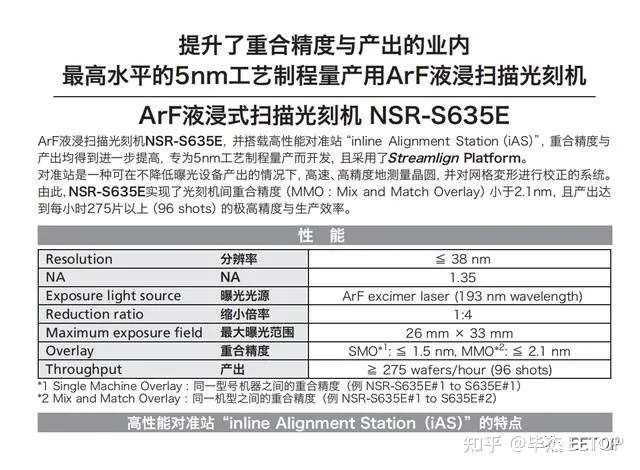
@FairAndUnbiased bro I'm waiting from you, @krautmeister @WTAN @foofy @tokenanalyst and others an analysis comparison, I know with spare info regarding the SMEE DUVL (like the MMO 2.5nm SMEE vs the 2.1nm of Nikon) but I like to know your views. :cool: Sorry for being a nuisance.
I am not too familiar with Nikon DUVL so i will look at SMEE vs ASML.

The stated MMO of SMEE DUVL is 2.5nm
The MMO of ASML 1980i is 2.5nm
The MMO/CMO of 2000i is 2.5nm
The MMO/CMO of 2050i is 2.5nm
The 2000i and 2050i have a ORION Alignment Sensor so the MMO is probably better than 2.5nm.

I would say that the SMEE 28nm DUVL is broadly equivalent to the 1980i.
Based on the SMEE MMO of 2.5nm which is similar to that of the 1980i, it should be able to do the 14nm process with Multi Patterning.
The 1980i is used by SMIC in China to produce 14nm ICs and the N+1(8nm) and N+2(7nm).
TSMC may have used the 1980i to produce their DUVL 7nm ICs.

SMEE will no doubt seek to improve the Overlay Accuracy of their DUVL so that it can match the latest NIKON DUVL in order to enable the production of 5nm ICs.
They should be able to achieve this as their MMO is already quite advanced by ASML and NIKON standards.
 

Attachments

  • Screenshot_20211027-004313.png
    Screenshot_20211027-004313.png
    489.7 KB · Views: 97

antiterror13

Brigadier
If Nikon can do it then in the future SMEE 28nm DUVL can, with the reports from my previous post of China Academy of Science had developed a 5nm laser lithography maybe they had plans and will work with SMEE to implement it in its future variants. I think SMEE or CETC may do a dual approach with its EUVL program and improving its DUVL. I'm speculating and forgive me for being an over enthusiast but a 5nm 3D DUVL chiplet will be competitive with the latest TSMC 3NM EUVL chip and if SMEE can improve the performance level comparable to NIKON and ASML NXT 2050i then it can buy some time for China IC especially Huawei, before the Chinese EUVL can be delivered in 2025.

From my friend @Oldschool

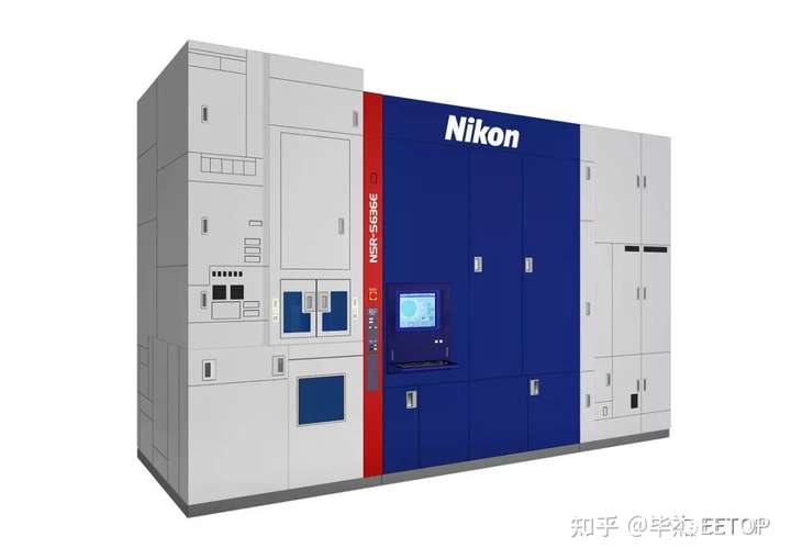
Nikon new immersion lithography can make 5nm, schedule to be on sale 2023.
Japan may not sell to CHina but this indicates DUV immersion can go beyond 7nm and down to 5nm.


Please, Log in or Register to view URLs content!


It can also process 5 nanometers! If you can't buy EUV, you can consider Nikon's new generation of ArF immersion lithography machine​

2021-10-24 13:06:36 Source: EETOP
Nikon recently announced that it is currently developing the next-generation NSR-S636E ArF immersion lithography machine, which will provide excellent stacking accuracy and ultra-high throughput to support the manufacturing of the most critical
Please, Log in or Register to view URLs content!
equipment. Product sales are planned to start in 2023.

v2-d20468f18d545e7f61ce6218491ca632_720w.jpg


With the acceleration of digital transformation (DX), there is an urgent need to process and communicate large amounts of data very quickly. In order to meet these requirements, high-performance
Please, Log in or Register to view URLs content!
imperative, and
Please, Log in or Register to view URLs content!
device technology is constantly evolving. At the same time, attention is paid to the miniaturization of circuit patterns and the development of 3D device structures.
NSR-S636E-line alignment station having enhanced (iAS), which is integrated between the coater / developer unit and a lithography scanner
Please, Log in or Register to view URLs content!
pre-
Please, Log in or Register to view URLs content!
module. S636E and iAS utilize complex multi-point alignment
Please, Log in or Register to view URLs content!
and advanced correction functions to enable equipment manufacturers to achieve the strict overlay accuracy required for 3D equipment structures while maximizing the productivity of immersion lithography machines. NSR-S636E is very suitable for cutting-edge
Please, Log in or Register to view URLs content!
manufacturing, including logic and storage devices, CMOS image sensor applications, etc.
More about the NSR-S636E parameters have not been announced, but from the previous generation S635E claims may have been produced 5nm
Please, Log in or Register to view URLs content!
of view, S636E should at least be a more efficient way of producing 5 nanometer
Please, Log in or Register to view URLs content!
, and our country can not buy this for
Please, Log in or Register to view URLs content!
For the lithography machine, it is a good choice.

v2-f76f75280682d6ad0d29004fb6454573_720w.jpg

Please, Log in or Register to view URLs content!

I'd bet SMEE will get it first before Nikon. Nikon would want to sell it to China, the big question is whether China would buy it ;)

Do you know what, once SMEE manage to produce it, ASML would rush selling its best DUV TWINSCAN NXT:2050i to China with a huge discount, not sure who would buy the Nikon one (if successful at all)
 

ansy1968

Brigadier
Registered Member
I'd bet SMEE will get it first before Nikon. Nikon would want to sell it to China, the big question is whether China would buy it ;)

Do you know what, once SMEE manage to produce it, ASML would rush selling its best DUV TWINSCAN NXT:2050i to China with a huge discount, not sure who would buy the Nikon one (if successful at all)
@antiterror13 Sir like @WTAN had stated SMEE and ASML had the same MMO at 2.5nm, SMEE had 2 years to improve its performance, with the help of SMIC, YMTC and even Huawei ICRD with end user feedback, I'm confident :cool: that what you post above WILL HAPPEN!;). Sir I'm going to repeat what @superdog once mentioned that a tool whatever sophistication can make a masterpieces if it's in the hand of a true master craftsman. And here SMEE had 3 masters to rely on while Japan Nikon need the cooperation from TSMC to produce a 28nm chip, A waste of resource and under utilization of the said machine.
 
Last edited:

ansy1968

Brigadier
Registered Member
An Addendum : TSMC will never used a Nikon DUVL to produced a 5nm chips cause they already master the technique using an EUVL and the investment had already been spend, So the latest Nikon DUVL 5nm capability is a nice to have advert, but who are their prospective customer? Or maybe the plan TSMC 28nm chip project is just a smoke screen for a more advance node like a 7nm or even a 5nm chip? Since Japan is paying will TSMC do it and had a competitor to their owned plan 6 FABS 7nm in Kaohsiung? The Nikon latest DUVL timeline of service is 2023, jive well with the projected operation of TSMC Japanese FAB, one can only wonder?
 

FairAndUnbiased

Brigadier
Registered Member
An Addendum : TSMC will never used a Nikon DUVL to produced a 5nm chips cause they already master the technique using an EUVL and the investment had already been spend, So the latest Nikon DUVL 5nm capability is a nice to have advert, but who are their prospective customer?
Intel is their sole public customer. The issue is this: the fabs pick winners and losers, and TSMC made the strategic choice of ASML long ago. So Nikon's fate became tied to Intel. With TSMC's sales and reinvestment, ASML was able to leap ahead of Nikon. Japan also has a tradition of vertical integration. What is Nikon's future? Maybe some Chinese companies can work with them, but right now they're in direct competition with SMEE for dry DUV lithography, packaging lithography, etc. Canon is doing very poorly when 15 years ago they were a market leader. Once SMEE gets immersion DUV, things look very grim for Nikon.

There are 3 reasons why things are grim for Nikon due to SMEE: 1. the semiconductor equipment market in Japan + Intel is much smaller than the rest of the world. 2. higher labor cost (still important due to the software component) 3. higher component cost in Japan vs China. The only way Nikon can survive is if they lower their costs and find a market. Maybe one that Japan is already highly integrated with. Maybe China. They can hire Chinese workers, buy Chinese components, and sell to Chinese companies. Maybe, Nikon can become Chinese in the end in all ways but the name.
 

ansy1968

Brigadier
Registered Member
From @Oldschool and my take its SMIC. ;)

China loongson CPU 12nm 龙芯3A5000

Please, Log in or Register to view URLs content!

目前,龙芯中科基于信息系统和工控系统两条主线开展产业生态建设,面向网络安全、办公与业务信息化、工控及物联网等领域与合作伙伴保持全面的市场合作,系列产品在电子政务、能源、交通、金融、电信、教育等行业领域已获得广泛应用。
www.loongson.cn
Please, Log in or Register to view URLs content!


The marking on the chip is CHN, this could be SMIC 12 nm process. I am not 100% sure. Either that or it's TSMC 12nm process in Nanjing

amp.scmp.com

Please, Log in or Register to view URLs content!

Shanghai wants to roll out 12-nanometre chips this year as part of an ambitious effort to strengthen domestic production and cut reliance on imported semiconductors.
amp.scmp.com
amp.scmp.com


daydaynews.cc

Please, Log in or Register to view URLs content!

OnDecember24thlastyear,龙芯releasedanewgenerationofproducts,3A4000/3B4000general-purposeCPUb
daydaynews.cc
daydaynews.cc
 
Status
Not open for further replies.
Top