Chinese semiconductor industry

Status
Not open for further replies.

jfcarli

Junior Member
Registered Member
Please, Log in or Register to view URLs content!
Huawei is being forced to become an octopus with 1000 tentacles. A few of those tentacles are bound to generate a handsome retribution.

Not only that, since they are one of the finest chip designers in the world they know exactly what is good and what needs to be done in order for themselves or a Chinese fab to become first class chip manufacturers.

Most important thing in the world is to know exactly what you want. And that, oh boy, Huawi definitely knows.
 

DarkStar

Junior Member
Registered Member
Actually the biggest threat to TSMC is Japan, EU and US.

TSMC 's business model relies on specialization/outsourcing, focusing exclusively on the foundries and manufacturing. The reason other companies got out of this segment is because of the level of cyclical capital investment and commitment necessary to stay on top of the industry.

With all the risks that recent US sanctions have initiated, EU, Japan and US are now all looking to replicate TSMC in their own turf. This will whittle away the focused specialization business model TSMC has built up in Taiwan. Over time, these spin outs may or may not come to threaten the profitability of the mothership in Taiwan.

Further, add to this the impending challenge from China in a few years....

This is how I think things looks for TSMC:
View attachment 75630
What do you expect when taiwan is led by a barren cat lady whose only hope for immortality is to go down in history as declaring taiwan independence?
anglo americans know that, which is why they're dangling recognition in front of the bitch whilst making off with the crown jewels of TSMC.
 

horse

Colonel
Registered Member
Huawei is being forced to become an octopus with 1000 tentacles. A few of those tentacles are bound to generate a handsome retribution.

This is a misconception because Hauwei was always an octopus with 1000 tentacles.

All they sold were switches for the telephone in their early days.

Then they sold everything related to the telecom network.

Then they sold phones, had a top chip design firm, they even made solar inverters. These businesses existed years before the Trump bans.

Once they built the 5G network, even more new business opportunities will present itself to Huawei.

The platform services from the cloud, and Huawei builds the absolute best server configuration for that too.

These were all Huawei projects in the works. They could not just snap their fingers and be number #1 in so many things.

Huawei number #1 in 5G technology.
Huawei number #1 in solar inverters.
Huawei number #1 in server farms.

Probably more.

No one pivots, and be number #1, just like that. It was all part of their business plans.

:)

ps. that is why they keep bringing up the phones that Huawei cannot make at the moment. It is for rhetorical comfort.

:p
 

Xizor

Captain
Registered Member

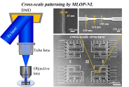
Photolithography: Super Resolution and High Efficiency Achieved Simultaneously​

2021-06-02
1628122520389.png

Photolithography has been an important patterning technique in past decades. The technique could utilize the high energy beam scanning, which are efficient to fabricate structures under nanometer scale without using expensive mask.

However, the patterning efficiency under the scale from nanometers to micrometers are extremely low. And it has restricted to its widely application.

To solve the contradiction of super resolution and efficiency in photolithography, Prof. ZHENG Meiling’s team from the Technical Institute of Physics and Chemistry (TIPC) of the Chinese Academy and Sciences (CAS) and Prof. DUAN Xuanming’s team from Jinan University have proposed a far-field maskless optical projective nanolithography (MLOP-NL) strategy.

This work is published in Nano Letters. The new protocol has enabled the cross-scale patterning with precise configuration could beyond the diffraction limit and achieve high efficiency.

In this study, scientists firstly solved the problem on the improvement of resolution beyond micrometer. The resolution can be improved through the optical nonlinearity, the chemical nonlinearity of nonchemical amplified (non-CA) resist, and the millions times repeating irradiation of femtosecond pulse. A minimum feature size of 32 nm, λ/12 super resolution breaking the optical diffraction limit, has been achieved in MLOP-NL process by a single exposure.

With the help of MLOP-NL strategy, it is flexible to achieve arbitrary cross-scale structures via simply changing the data of desired configuration. Furthermore, patch production could be performed by only repeating the process. Consequently, MLOP-NL technique provides a powerful tool allowing for achieving cross-scale patterns with both large-scale and precise configuration architectural feature.

The work is highly possible to open up a new avenue for the high efficient lot manufacturing with the further development of higher frequency laser and rapid responsive stage industry. It will also show potentials to researchers working in diverse fields of nanoscience and nanotechnology, including nanodevices, nanostructures, and nanolithography.

This work is supported by the National Key R&D Program, and the Natural Science Foundation of China.

Please, Log in or Register to view URLs content!
 

WTAN

Junior Member
Registered Member
Please, Log in or Register to view URLs content!
This lack of 5G RF Chips is a temporary issue for Huawei.
Hisilicon used to design their own 5G RF Chips and had them manufactured in Taiwan by WIN Co.
Huawei will probably be manufacturing their own 5G RF Chips when their own FAB is ready.
5G RF Chips are made using the 14nm or 28nm Process so this should not be a big issue for Huawei.
 
Status
Not open for further replies.
Top