Chinese semiconductor industry

Status
Not open for further replies.

gelgoog

Lieutenant General
Registered Member
Intel has had 10nm for years already. It is used in mobile processors. Their problem is they couldn't fab it at enough yield, so they did not have the production capacity and low manufacturing cost to use it in desktop processors.
AMD solved this by using chiplets and reducing the amount of high density die space the processor used.
 

nlalyst

Junior Member
Registered Member
Jesus. Just read this.
Please, Log in or Register to view URLs content!


And now read this.
Please, Log in or Register to view URLs content!


This is what TSMC was doing in the year SMIC was founded in 2000.
Please, Log in or Register to view URLs content!


In 2001 that VIA C3 was being sold in the market.
Please, Log in or Register to view URLs content!

And you claim this crock of shit.


In prior posts you looked at graphics chips like 3Dfx and NVIDIA. Back then graphics chips were much less sophisticated than CPUs and used much older manufacturing processes. So of course they weren't manufactured with the latest and greatest process. Back then the graphics chip did not do compute, it was not a general purpose processor, it only rendered polygons and sometimes textures. 3Dfx didn't even have 2D processing in it to make it even less complex to manufacture.
So this means you couldn't find a TSMC 180nm product before 2000 and are moving the goalpost to 130nm?
 

nlalyst

Junior Member
Registered Member
Here's another
Please, Log in or Register to view URLs content!
from February 2004, confirming that SMIC had 180nm production as early as 2002. In 2003 it had both 180nm and 130nm production:

SMIC also made rapid gains in introducing new process technology. At the end of 2002, the company earned nothing from 0.15-micron and 0.13-micron manufacturing processes and only 4.7 percent of its wafers used 0.18-micron technology. But by the end of last year, 0.18-micron accounted for 22 percent of wafers, 0.15-micron for 9.9 percent and 0.13-micron for 11.8 percent.
So, by moving to 130nm SMIC closed the gap to 2 years? Was the US government right after all? A report from 2002 indicated that in the SMIC collaboration with Texas Instrument, SMIC was offering its indigenous 130nm technology:
Semiconductor Manufacturing International Corp. (SMIC), Shanghai, has a foundry alliance with Texas Instruments on DSP chips using 130-nanometer process technology. That state-of-the-art semiconductor node would make a mockery of the current U.S. control limit below quarter-micron processing.

A TI spokesman confirmed that the chipmaker has a memorandum of understanding with SMIC for 130nm node chips, with product qualification in 2003. He said TI will partially produce the active layers of the chips at its DMOS 8-inch fab in Dallas, and ship them to SMIC which will complete the metal interconnect layers using its own 130nm technology.

Again, reference to how this alarmed TSMC with mention of the Broadcom chip at 0.18 micron they used as proof:
Such a rapid ramp-up is part of what drew the attention of TSMC. In its lawsuit, the Taiwan-based foundry alleged that SMIC has lured away key personnel and tapped their expertise of TSMC processes to accelerate its learning curve.

The suit further alleges that “outright theft” of IP has enabled SMIC “to price its products at a substantial discount to what would have otherwise been possible had SMIC incurred its own research-and-development and ramp-up expenses.”

Specifically, TSMC claims that some of those patents were used to fabricate a 0.18-micron chip for Broadcom Corp. Examination of the chip “revealed identical or nearly identical structures….that TSMC believes could only have been fabricated using TSMC's proprietary process steps,” the lawsuit says
 
Last edited:

jfcarli

Junior Member
Registered Member
True, you don't actually need software engineers who have past experience with working on EDA systems. You just need a small core of domain knowledge experts that thoroughly understand the problem space. Whatever domain knowledge the senior engineers would need to know can be knowledge transfered from your core group of experts, most ICs would need only limited amounts of domain specific knowledge.

However, this process still takes time, and throwing more engineers at the problem will not speed it up further. There is a popular adage in the industry that goes along the lines of, "Nine mothers cannot have one baby in one month." Would expect it would take a few years, but still very fast relative to other technical challenges such as developing EUV machines, node processes, and light sources.
I realize the equipment is by far the most difficult to obtain. I understand also that one can still use the EDA software already purchased, or, maybe, pirated copies. On the other hand, I do understand also that China is still short in EDA and eventually China MUST master EDA, thus being fully in control of the software without lagging behind in updates.

I have been a coder, a systems analyst and a client. As an analyst I know for sure that if you use TOP DOWN systems analysis, and above all KNOW WHAT YOU WANT, you can get nine mothers to give birth to a baby in one month.

I believe the people who best know what to do with EDA are the people at Hisilicon and for sure they are not terribly busy right now. If they join efforts with the EDA developers, provided they can lay hands on a competent chief systems analyst/manager, they might be able to get 18 mothers to give birth to the baby in 15 days, instead of one month.
 

gelgoog

Lieutenant General
Registered Member
So this means you couldn't find a TSMC 180nm product before 2000 and are moving the goalpost to 130nm?

What a crock of shit.
Please, Log in or Register to view URLs content!

Please, Log in or Register to view URLs content!

ManufacturerTSMC
First Introduction Oct 13, 1998 (PR166, PR233, PR266)
May 26, 1999 (0.25 µm PR333 and PR366)
May 26, 1999 (0.18 µm PR333 and PR366)

TSMC also manufactured a die shrink of the Cyrix M-II processor at 180nm after it was bought by VIA.

I am still waiting for your SMIC manufactured chips. If you believe your previous posts SMIC copied TSMC's 180nm process, yet they were manufacturing chips at 180nm while TSMC still had 250nm. Some logic there.
 
Last edited:

nlalyst

Junior Member
Registered Member
More background behind SMICs rapid catch-up to TSMC in the early 2000s, from EE times:

Mora was the subject of intense scrutiny in TSMC’s recent suit with SMIC. In 2000, TSMC acquired Worldwide Semiconductor Manufacturing Corp. (WSMC), a Taiwan-based foundry. Chang was the president of WSMC, Mora was vice president of operations and Katy Liu was the manager of Q&A. Following the deal, Chang, Mora and Liu become employees of TSMC.

Shortly after that event, Chang left TSMC to form SMIC, TSMC alleged. Mora was the operations manager of TSMC’s Fab 8B, until he resigned from TSMC and joined SMIC in May of 2000, TSMC alleged.

Then, according to TSMC, Mora, who was working at SMIC, allegedly sent e-mails to Liu, who was still working at TSMC. In the e-mail, Mora allegedly requested Liu to ”pull out some of the information from WSMC/TSMC.”

The ”information” that was allegedly taken was TSMC’s secret sauce, including its latest 180-nm technology, among other processes, at that time, according to TSMC. Liu resigned from TSMC in early 2001.

TSMC originally filed suit in December of 2003, about three months before SMIC’s IPO. That suit claimed SMIC had systematically pilfered TSMC trade secrets by hiring hundreds of its engineers and asking a few senior people to take information with them as they left. The two sides settled about a year later.

In 2006, TSMC sued SMIC for breach of a settlement agreement, breach of promissory notes, and trade secret misappropriation. TSMC’s complaint accused SMIC of “massive corporate espionage” and claimed that SMIC “lavishly copied the information it stole from TSMC, word for word, and even typographical error for typographical error.”

TSMC alleged that SMIC incorporated TSMC trade secrets in the manufacture SMIC’s 0.13 micron or smaller process products. TSMC further alleged that the alleged breach terminated TSMC’s patent license made ineffective the covenant not to sue with respect to SMIC’s larger process products.

After the liability phase of the trial, the jury last week found in favor of TSMC on 61 of 65 trade secret claims. Beyond the verdict, what’s next for SMIC?
 

krautmeister

Junior Member
Registered Member
If Huawei sold the design/technology 3nm to Unisoc, or Xiaomi/Oppo hence it is not down the drain.
The same rules apply to all China companies when it comes to nodes <=14nm. If Unisoc were able to design a competitive SoC at 3nm, first they wouldn't be able to without using US EDA tools, and even if they could with China EDA, they would be restricted via the US content rules on lithography tools.
 

nlalyst

Junior Member
Registered Member
What a crock of shit.
Please, Log in or Register to view URLs content!

Please, Log in or Register to view URLs content!

ManufacturerTSMC
First Introduction Oct 13, 1998 (PR166, PR233, PR266)
May 26, 1999 (0.25 µm PR333 and PR366)
May 26, 1999 (0.18 µm PR333 and PR366)

TSMC also manufactured a die shrink of the Cyrix M-II processor at 180nm after it was bought by VIA.

I am still waiting for your SMIC manufactured chips. If you believe your previous posts SMIC copied TSMC's 180nm process, yet they were manufacturing chips at 180nm while TSMC still had 250nm. Some logic there.
That's a good find.

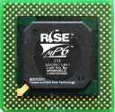
However, I found some contradictory sources claiming that the 180 nm chip never reached the market and only a few engineering samples were ever made:
Please, Log in or Register to view URLs content!

The date of manufacture is listed as 12th week of 2000. If the only a few engineering samples were ever made, it doesn't seem likely there would've been another run in 1999. Here's a screenshot:

mp6.jpg

Also claimed here that it was never released:
Please, Log in or Register to view URLs content!
 

krautmeister

Junior Member
Registered Member
So the bottleneck is really China's lack of advanced lithography equipment.

Once these equipment are available it would be only a matter of configuring the Chinese EDA software to work with them with little change to the software at the higher level of chip design work. The biggest hurdle still comes back to the equipment hardware.
EDA is only 1 bottleneck but mainly because domestic EDA can't catch up without full access to leading edge fabs and equipment which then restricts adoption, which then restricts profits, more R&D, etc. So, the lithography equipment is a much bigger bottleneck. For China, the entire domestic semiconductor supply chain has to advance at the same pace, otherwise the domestic laggards will become a bottleneck.
 

nlalyst

Junior Member
Registered Member
I am still waiting for your SMIC manufactured chips. If you believe your previous posts SMIC copied TSMC's 180nm process, yet they were manufacturing chips at 180nm while TSMC still had 250nm. Some logic there.
Of course I believe it. SMIC was found guilty for stealing trade secrets and breaching the terms of the 2005 settlement:
Please, Log in or Register to view URLs content!


SMIC agreed to settle a week later:
Please, Log in or Register to view URLs content!
 
Status
Not open for further replies.
Top