Chinese semiconductor industry

Status
Not open for further replies.

Hendrik_2000

Lieutenant General
I guess they are thinking of dumping ARM
Please, Log in or Register to view URLs content!
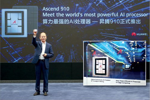
rotating chairman Eric Xu confirmed Friday Huawei is exploring alternatives to chip design software from current market leaders. The tech giant unveiled a powerful AI processor
Please, Log in or Register to view URLs content!
to grow the cloud services market and accelerate industrial upgrade in China.

ECsrW2kUcAAIt2c.jpg
 

Tam

Brigadier
Registered Member
I don't know if this was already posted. Lenovo is already using some chips from this company.

Please, Log in or Register to view URLs content!


Chinese-Produced Zhaoxin KX-6000 CPUs Purportedly Match Intel's Core i5-7400


Excerpts:

"Late last year, the China-based processor designer Zhaoxin Semiconductor (jointly owned by the Shangai government and VIA Technologies, another semiconductor corporation) promised its upcoming octa-core CPUs based on the 16nm node from TSMC would be able to match Intel's quad-core i5 processors, and today is that day: the newly-announced KX-6000 CPUs are said to deliver performance on par with the Core i5-7400, yet supposedly pull off the feat at a mere 3 GHz. And they support Windows. While this level of performance may not seem very impressive, it is actually a very significant development for a few reasons."

"The Core i5-7400 isn't Intel's fastest desktop CPU by any means (not even when it launched in 2017), but it is one of the fastest desktop CPUs made by any company today. Even AMD's first-gen Ryzen CPUs struggled against it in single-threaded workloads."


zhaoxin_chips_678_678x452.jpg
 

Tam

Brigadier
Registered Member
Chinese vendor creates GPU targeting nVidia GTX 1080. This company started life making GPUs for military displays.

Please, Log in or Register to view URLs content!


Excerpt.

"A post
Please, Log in or Register to view URLs content!
has additional information. Currently, the JM7200 is said to offer performance equivalent to the GeForce GT 640, albeit in a much lower power envelope — 10W, supposedly, compared with the 50W Nvidia specced for that card. We’d like to see that claim independently verified. The OEM variant of the GT 640 was a Fermi-based part built on 40nm, but that chip had a 65W TDP. The 50W variant was a Kepler-derived part built on 28nm — the same process node Jingjia Micro uses. The JM part also supposedly has 4GB of RAM, while the GT 640 50W version had just 1GB of GDDR5.

The JM9231 and JM9271 are supposedly the first fully programmable GPUs that Jingjia Micro has developed; there are references to the previous JM5400 and JM7200 families being based on fixed-function rendering pipelines. These limitations wouldn’t fly under modern APIs for Windows, but the company started life as a military GPU vendor, and such applications obviously have very different requirements for APIs and product certification."

24jingjia-micro-jm9271.jpg Jingjia-Micro-Chart-640x478.png
 

Hendrik_2000

Lieutenant General
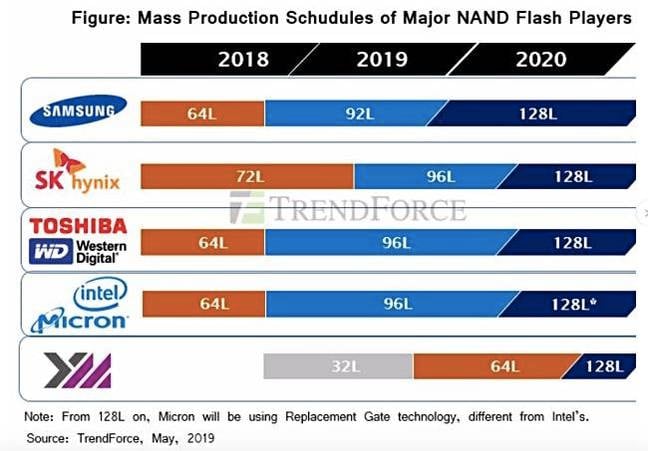
China start mass producing home grown memory chip via xyz. Huawei should be glad with this development. Is NAND for smart phone ?

On September 2, 2019, Wuhan, China, Ziguang Group's Yangtze River Storage Technology Co., Ltd. (hereinafter referred to as “Yangtze Storage”) announced on the eve of IC China 2019 that the company has begun mass production of 64-layer 256 Gb TLC 3D based on Xtacking® architecture. NAND flash memory 1 meets the needs of mainstream market applications such as solid state drives and embedded storage.

As China's first 64-layer 3D NAND flash memory, the product will be unveiled at the IC China 2019 Ziguang Group booth. Yangtze River Storage 64-layer 3D NAND flash wafers Yangtze River Storage 64-layer 3D NAND flash memory is the world's first flash memory product based on Xtacking® architecture and mass production, with the highest storage density of the same generation. Xtacking® enables peripheral circuits and memory cells to be fabricated separately on two separate wafers, which facilitates the selection of more advanced manufacturing processes.

When the two wafers are completed, the innovative Xtacking® technology allows two wafers to be bonded through billions of Vertical Interconnect Channels (VIAs) in a single processing step. Compared to traditional 3D NAND flash architectures, Xtacking® delivers faster I/O transfer speeds, higher storage densities and shorter time-to-market. As an integrated device manufacturer (IDM - Integrated Device Manufacturer), Changjiang Storage is committed to providing complete storage solutions and services to customers around the world, and plans to introduce solid-state hard drives, UFS and other products with integrated 64-layer 3D NAND flash memory to meet the data center.

And the needs of enterprise server, PC and mobile device manufacturers. Changjiang Storage has always attached importance to the independent research and development and innovation of core technologies. The successful development of Xtacking® technology and the mass production of 64-layer 3D NAND flash memory indicate that Changjiang Storage has successfully embarked on a new high-end chip design and manufacturing innovation. In the future, Changjiang Storage will continue to invest in research and development resources to make each generation of products have strong market competitiveness and better meet the needs of global customers through the iteration of technology and products. Cheng Weihua, co-chief chief technology officer and senior vice president of technology research and development center of Changjiang Storage, said: "By introducing Xtacking® architecture into mass production, it can significantly improve product performance, shorten development cycle and manufacturing cycle, and promote the market of high-speed and large-capacity storage solutions.

Rapid development." Cheng Weihua also mentioned, "With the advent of 5G, artificial intelligence and ultra-large data center era, the demand for the flash memory market will continue to grow. The mass production of 64-layer 3D NAND flash memory products will be healthy for the global memory market. Development injects new impetus.” 3 Notes: 1 Each bare chip has a storage capacity of 256 gigabits, and each memory cell has three-dimensional three-dimensional flash memory. 2Specially refers to the 64/72 layer 3D NAND flash memory that has been listed in the industry. 3 Yangtze River Storage, YMTC, YM Graphic Logo and Xtacking are trademarks of Changjiang Storage Technology Co., Ltd. or its molecular companies in China and/or other countries

2019年9月2日,中国武汉,紫光集团旗下长江存储科技有限责任公司(以下简称“长江存储”) 在IC China 2019前夕宣布,公司已开始量产基于Xtacking®架构的64层256 Gb TLC 3D NAND闪存①,以满足固态硬盘、嵌入式存储等主流市场应用需求。作为中国首款64层3D NAND闪存,该产品将亮相IC China 2019紫光集团展台。

5d6c7d5db855a.jpg

长江存储64层3D NAND闪存晶圆

长江存储64层3D NAND闪存是全球首款基于Xtacking®架构设计并实现量产的闪存产品,拥有同代产品②中最高的存储密度。Xtacking®可实现在两片独立的晶圆上分别加工外围电路和存储单元,这样有利于选择更先进的制造工艺。当两片晶圆各自完工后,创新的Xtacking®技术只需一个处理步骤就可通过数十亿根垂直互联通道(VIA)将两片晶圆键合。相比传统3D NAND闪存架构,Xtacking®可带来更快的I/O传输速度、更高的存储密度和更短的产品上市周期。

作为集成器件制造商(IDM - Integrated Device Manufacturer),长江存储致力于为全球客户提供完整的存储解决方案及服务,并计划推出集成64层3D NAND闪存的固态硬盘、UFS等产品,以满足数据中心,以及企业级服务器、个人电脑和移动设备制造商的需求。

长江存储一贯重视核心技术的自主研发和创新,Xtacking®技术的研发成功和64层3D NAND闪存的批量生产标志着长江存储已成功走出了一条高端芯片设计制造的创新之路。

今后,长江存储仍将持续投入研发资源,以通过技术和产品的迭代,使每一代产品都具备强劲的市场竞争力,更好地满足全球客户的需求。

长江存储联席首席技术官、技术研发中心高级副总裁程卫华表示:“通过将Xtacking®架构引入批量生产,能够显著提升产品性能,缩短开发周期和生产制造周期,从而推动高速大容量存储解决方案市场的快速发展。”程卫华还提到,“随着5G,人工智能和超大规模数据中心时代的到来,闪存市场的需求将持续增长。长江存储64层3D NAND闪存产品的量产将为全球存储器市场健康发展注入新动力。” ③

注:

①每颗裸芯片的存储容量为256千兆字位,每个存储单元为三个字位的三维闪存。

②特指截止目前业界已上市的64/72层3D NAND 闪存。

③长江存储、YMTC,YM图形徽标和Xtacking是长江存储科技有限责任公司或其分子公司在中国和/或其他国家/地区的商标。
 

Hendrik_2000

Lieutenant General
Via JSCh
Semiconductor industry on steady track despite outbreak
By Ma Si | China Daily | Updated: 2020-02-20 09:16

5e4ddde1a31012820654130b.jpeg

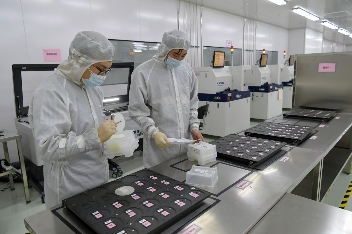
Employees perform tests on semiconductor chips at the production facility of a Nanchang, Jiangxi province-based high-tech company on Feb 13. [Photo/Xinhua]

Epidemic will not alter the long-term momentum of the sector, says a report


The novel coronavirus outbreak will have a limited impact on China's semiconductor industry since most local wafer manufacturing plants are operating normally and chip design companies can choose remote work to mitigate the fallout from the epidemic, the companies concerned and analysts said.

The chip packaging and test business may be affected to some extent due to the labor shortage, they added.

Semiconductor Manufacturing International Co, the top contract chip manufacturer in the Chinese mainland, said on Friday the company will double its capital spending and expects revenue to grow more than 10 percent this year despite the epidemic.

Zhao Haijun, co-CEO of SMIC, said at an earnings call that all of the company's factories which are mainly located in Shanghai, Beijing and Tianjin are running at full capacity.

The comments came after the company had organized a work group before the Spring Festival holiday to ensure that plants could stay open, while protecting the safety of employees and following government regulations.

"SMIC needs to ensure that factory production runs 365 days a year, 24 hours a day to meet customers' fabrication needs," the company said in a statement.

Fang Jing, chief electronics analyst at Cinda Securities, said most wafer manufacturing plants are dust-free, which makes them less vulnerable to virus infection. It is also a common practice in the industry to keep the highly-automated plants running all year round.

Located in the badly hit city of the contagion outbreak, the Wuhan, Hubei province-based Yangtze Memory Technologies Co Ltd also said its production and operations are proceeding normally and in an orderly manner.

The company has enacted certain isolation measures and partitions to ensure the safety of employees. It is also striving to coordinate with multiple sides to maintain the supply of industrial production materials and logistics services to ensure the sustainability of its businesses, YMTC said in a statement.

Most chip design companies have also resumed operations, with most employees working remotely from their homes.

Shanghai-based HiSilicon, the chip arm of Huawei Technologies Co, said it has already restarted operation. It added that it is pouring resources into maintaining normal operations while preventing its employees from getting infected by the virus.

Unisoc Technologies Co, a core chip subsidiary of Tsinghua Unigroup, said its employees have also gone back to work, with its plants running non-stop since the Lunar New Year holiday.

Though logistics services have been affected by the novel coronavirus outbreak, the company said that it is working hard to solve the problem.

Allwinner Technology, a chip design company based in Zhuhai, Guangdong province, also said it has resumed operations, and shipped a batch of new products last week.

Analysts said the epidemic is partly harming the chip packaging business.

Fang of Cinda Securities said unlike wafer manufacturing plants which run non-stop year round, chip packaging factories usually are closed during the Spring Festival for maintenance work on their equipment.

Taiwan-based chip packing and test company AES said recently the lack of available labor is the biggest problem for its mainland branches. Traffic restrictions during the outbreak make it difficult for many employees who have gone home for the holidays to return to work.

Even if they manage to return, they have to go through the process of health examinations and a seven to 14-day quarantine period.

Another factor is that the first quarter is usually the off-season for the semiconductor industry, which provides a cushion of time for its companies.

AES said despite all the difficulties, 60 to 70 percent of its employees in its plants in the Chinese mainland were on duty during the Spring Festival holiday.

By the end of February, the proportion is expected to reach 80 percent to 85 percent, and by the end of the first quarter, all of its employees will have returned to work, the company said.

JCET Group, another Chinese chip packaging and test company, said earlier this month that its production and operations remain stable. Due to abundant orders during the Spring Festival, only few employees of the company's plant in Jiangyin, Jiangsu province, had gone home for the holidays.

The company said it currently has enough stocks of industrial production material to meet demand. It added it is working closely with government agencies and supply partners to see how to get more raw materials to meet future demand.

Western Securities said in a report that the outbreak will not alter the long-term, strong momentum of China's semiconductor sector.

The upcoming large-scale rollout of 5G networks and the push of China's tech giants to cultivate local chip suppliers have combined to inject fresh vitality into the industry.

China will still build its 5G networks this year. The demand may be delayed by the virus, but it will not vanish, Fang of Cinda Securities explained.
 

Hendrik_2000

Lieutenant General
Via j20blackdragon cheaper 5G smartphone is coming and bad new for Qualcomm
Please, Log in or Register to view URLs content!


UNISOC Unveils T7520 SoC for 5G Smartphones: Octa-Core, 6nm EUV

by Anton Shilov on March 4, 2020 10:00 AM EST

UNISOC, formerly Spreadtrum Semiconductor, has announced its first mobile application processor with an integrated 5G modem. Dubbed the T7520, the SoC also happens to be one of the world’s first chips to be made using TSMC’s 6 nm process technology, which uses extreme ultraviolet lithography (EUVL) for several layers.

The UNISOC T7520 application processor packs four high-performance Arm Cortex-A76 cores, four energy-efficient Arm Cortex-A55 cores, as well as an Arm Mali-G57 GPU with a display engine that supports multiple screens with a 4K resolution and HDR10+. Furthermore, the SoC integrates a new NPU that is said to offer a 50% higher TOPS-per-Watt rate than the company’s previous-generation NPU. In addition, the chip features a four-core ISP that supports up to 100 MP sensors and multi-camera processing capability. Finally, the AP also features the company’s latest Secure Element processor that supports ‘most of crypto algorithms’ and can handle compute-intensive security scenarios, such as encrypted video calls.

One of the key features of the UNISOC T7520 is of course its integrated 2G/3G/4G/5G-supporting modem, which supports 5G NR TDD+FDD carrier aggregation, as well as uplink and downlink decoupling for enhanced coverage. All told, the T7520's modem is designed to offer peak uplink speed of 3.25 Gbps.

The high level of integration of the T7520 SoC is designed to enable smartphone manufacturers to build more reasonably priced 5G handsets, which will inevitably increase their popularity and adoption of the technology. Meanwhile, usage of TSMC’s 6 nm fabrication technology (known as N6) should allow UNISOC to make the AP for less than compared to non-EUV fabrication processes.

UNISOC did not announce when it plans to start shipments of its T7520 application processor, though it is reasonable to expect it to become available this year.
 

Hendrik_2000

Lieutenant General
Via Antonius
Please, Log in or Register to view URLs content!

SMIC 7nm process to be introduced in Q4 with 20% performance improvement
February 27, 2020
Please, Log in or Register to view URLs content!
1
The 7nm process of Semiconductor Manufacturing International Corporation (SMIC), China's most advanced and largest foundry, will begin small-scale production in the fourth quarter, according to kkj.cn.

Compared with 14nm, SMIC's N+1 process improves performance by 20%, reduces power consumption by 57%, reduces logic area by 63%, and reduces SoC area by 55%, the report cited Dr. Liang Mengsong, co-CEO of SMIC, as saying.

TSMC and Samsung will mass produce 5nm processes this year, and China's advanced processes are still catching up.

The largest wafer foundry, SMIC, mass-produced a 14nm process at the end of last year, which brought 1% of revenue and revenue of $7.69 million, but this process technology can already meet 95% of domestic demand.

The 14nm and improved 12nm processes are SMIC's first-generation FinFET processes. They are also developing more advanced N+1 including N+2 FinFET processes, which are equivalent to low-power, high-performance versions of the 7nm process.

After N+1, there will also be N+2. These two processes perform similarly in terms of power consumption. The difference lies in performance and cost. N+2 is obviously oriented towards high performance and the cost will increase.

As for the EUV lithography machine that has attracted much attention, Liang Mengsong said that under the current environment, N+1 and N+2 generation processes will not use the EUV process. After the equipment is ready, the N+2 process may have several photomasks. With EUV, the subsequent process will switch to EUV lithography on a large scale.

Now the most important thing is when SMIC will be mass-produced at 7nm. The latest news says that SMIC's N+1 FinFET process has been introduced by customers (but no customer list has been announced). Small-scale production will begin in the fourth quarter of this year, earlier than previously reported.

In order to accelerate advanced process capacity, SMIC's capital expenditure will reach US $ 3.1 billion this year (the company's annual revenue is only around US $3 billion), of which US $2 billion will be used for SMIC's 12-inch wafer fab in Shanghai and US $500 million At a 12-inch wafer fab in Beijing.
 

manqiangrexue

Brigadier
Via Antonius
Please, Log in or Register to view URLs content!

SMIC 7nm process to be introduced in Q4 with 20% performance improvement
February 27, 2020
Please, Log in or Register to view URLs content!
1
The 7nm process of Semiconductor Manufacturing International Corporation (SMIC), China's most advanced and largest foundry, will begin small-scale production in the fourth quarter, according to kkj.cn.

Compared with 14nm, SMIC's N+1 process improves performance by 20%, reduces power consumption by 57%, reduces logic area by 63%, and reduces SoC area by 55%, the report cited Dr. Liang Mengsong, co-CEO of SMIC, as saying.

TSMC and Samsung will mass produce 5nm processes this year, and China's advanced processes are still catching up.

The largest wafer foundry, SMIC, mass-produced a 14nm process at the end of last year, which brought 1% of revenue and revenue of $7.69 million, but this process technology can already meet 95% of domestic demand.

The 14nm and improved 12nm processes are SMIC's first-generation FinFET processes. They are also developing more advanced N+1 including N+2 FinFET processes, which are equivalent to low-power, high-performance versions of the 7nm process.

After N+1, there will also be N+2. These two processes perform similarly in terms of power consumption. The difference lies in performance and cost. N+2 is obviously oriented towards high performance and the cost will increase.

As for the EUV lithography machine that has attracted much attention, Liang Mengsong said that under the current environment, N+1 and N+2 generation processes will not use the EUV process. After the equipment is ready, the N+2 process may have several photomasks. With EUV, the subsequent process will switch to EUV lithography on a large scale.

Now the most important thing is when SMIC will be mass-produced at 7nm. The latest news says that SMIC's N+1 FinFET process has been introduced by customers (but no customer list has been announced). Small-scale production will begin in the fourth quarter of this year, earlier than previously reported.

In order to accelerate advanced process capacity, SMIC's capital expenditure will reach US $ 3.1 billion this year (the company's annual revenue is only around US $3 billion), of which US $2 billion will be used for SMIC's 12-inch wafer fab in Shanghai and US $500 million At a 12-inch wafer fab in Beijing.
Holy smokes that's fast (if it isn't severely delayed)! Didn't Western "experts" say it would take China more than 10 years to get close to here? At this rate, they might hit 3nm before Samsung/TSMC!

When Chinese semiconductor tech comes into full parity with the best of the world, China should really host a national party with "Thank You Donald Trump" banners everywhere, this time actually with more attendance than any rally or welcome he's ever attended. I wanna see if he tries to spin it as a positive of how much China loves him! LOL
 
Status
Not open for further replies.
Top