Chinese semiconductor industry

Status
Not open for further replies.

horse

Colonel
Registered Member
Why can't I shake off the feeling/fear that they're trying to just kill us all one day.
That is just the America psy-ops.

The idea is to make people cautious, so that they will not act independently. Americans would try to manipulate their rivals into thinking, then doing what the American want. Essentially it is a form of mind control.

American psy-ops is very bad.

Very good psy-ops is the Chinese wife.

You never seen real psy-ops until you have gotten married.

:oops: :D
 

horse

Colonel
Registered Member
Hi bro, Happy Chinese New Year and good health to you and your family. from my recollect the info of @WTAN from last year all had proven correct, now the recent news only confirm what we already know that the 14nm domestic line is ready couple with SMEE 28nm DUVL we are on a crucible of self sufficiency.
If the process for the 14nm is the same with 7nm Chemical and material wise, then that jump will not be as difficult as the SMEE 28nm DUVL can able to produce it using multiple patterning. @WTAN info on SMIC N+1 (8nm)slated for April mass production all pointed to a domestic line since they are ban from producing anything below 10nm. The year is still young and I'm waiting for info regarding SMIC N+2 from @WTAN and I think with the urgency, I wouldn't be surprise they can pull this of by late 2021.;)
Hi ansy1968, happy new year, good health, look for big fortune in Ox year.

Let's see what this year brings.

:D
 

quantumlight

Junior Member
Registered Member
That is just the America psy-ops.

The idea is to make people cautious, so that they will not act independently. Americans would try to manipulate their rivals into thinking, then doing what the American want. Essentially it is a form of mind control.

American psy-ops is very bad.

Very good psy-ops is the Chinese wife.

You never seen real psy-ops until you have gotten married.
:oops: :D
Yes its part of the 5th Generational information warfare the US is leveraging its media, platforms, etc to full effect

psy-ops or not, China needs to have sufficent nukes.... the cost/economic arguement is moot... whats the point of saving money if you are dead... was the genocide and extermination of native americans also merely a psy-ops?

at some point when the rubber meets the pavement you have to have real physical reality backing up the bluffs...

America cant out-psyops a 10,000+ Chinese nuke stockpile unless they think they can convince China to forgive and forget after first doing a strategic strike on the mainland China...

Only power is real, at the end of the day, China arming up and gaining massive deterrence will free it to pursue its intetests on its terms

The real psyops is America trying to psyops the psyops and get China to back down from increasing its nuclear stockpile
 

Oldschool

Junior Member
Registered Member
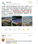
Huawei applying patent for photonic chip and established a fab for such.
Photonic chip using light instead of electron. In the past photonic chip used for transmission but huawei patent photonic chip is logic and calculation. Unlike traditional semiconductor, photonic chip do away with traditional lithography.

In the not distant future, Huawei will have a Photonic CPU.

1613338166618.png
1613338265599.png


而就在近日,华为海思再次带来了全新的芯片专利技术,根据公开的资料显示,这次华为所申请的芯片专利被命名为“光计算芯片、系统及数据处理技术”,这项全新的芯片专利技术,似乎也在表明华为目前着重发展的目标,例如光计算、系统、数据处理,并且这次华为所带来的芯片产品,并非是目前的传统电子芯片年产品,而是全新的光子芯片产品,而电子芯片、光子芯片之间最大的区别,就是目前电子芯片发展已经受到了物理极限的束缚,而光子芯片则不会受到爱摩尔定律天花板的限制,相对于传统的电子芯片产品,拥有更快的运算速度、更加理想的功耗表现,所记光子芯片也被誉为来自于未来的芯片产品。


And just recently, Huawei HiSilicon once again brought a brand-new chip patent technology. According to public information, the chip patent that Huawei applied for this time was named "Optical Computing Chip, System and Data Processing Technology." The patented technology of chips also seems to indicate Huawei’s current development goals, such as optical computing, systems, and data processing, and the chip products that Huawei brings this time are not the current traditional electronic chip products, but brand new Photonic chip products, and the biggest difference between electronic chips and photonic chips is that the development of electronic chips has been constrained by physical limits, while photonic chips will not be restricted by the ceiling of Love Moore's law. Compared with traditional electronic chip products , With faster computing speed and more ideal power consumption performance, the recorded photonic chip is also known as a chip product from the future.
1613338652261.png
1613338704741.png
1613338826283.png
 
Last edited:

horse

Colonel
Registered Member
In the not distant future, Huawei will have a Photonic CPU.
This "Optical Computing Chip, System and Data Processing Technology," I had read something about that patent, but did not understand it.

Now when you say it is a photonic, then it makes sense and I understand generally what they are doing.

This is totally kick ass!

Not only they are research and doing this new method, they filed a patent.

They filed a patent because they already enough about it, how it works!

That is amazing!

Tech war? What tech war!? Come and get it Uncle Sam.

:D :oops: :p
 

Oldschool

Junior Member
Registered Member
This "Optical Computing Chip, System and Data Processing Technology," I had read something about that patent, but did not understand it.

Now when you say it is a photonic, then it makes sense and I understand generally what they are doing.

This is totally kick ass!

Not only they are research and doing this new method, they filed a patent.

They filed a patent because they already enough about it, how it works!

That is amazing!

Tech war? What tech war!? Come and get it Uncle Sam.

:D :oops: :p
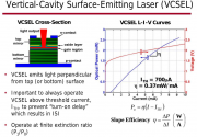
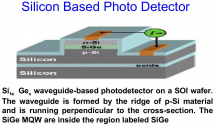
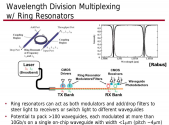
Good thing is photonic manufacturing process is leveraging alot from semiconductor silicon process. They can build their laser, detectors, waveguide, logic in silicon. They don't have really invent anything new manufacturing process wise. Traditional photonic chip is just used for speeding up of transmission and coupled to semiconductor CPU.
And Huawei will be the first one to build such fab to make photonic CPU. All the process manufacturing engineers Huawei hired recently I think are for this project and make this fab up and running.

Traditional semiconductor IC process, they just farm out to Shanghai ICRD. They are already late to the party better off going different route


Maybe can say goodbye to TSMC and SMIC one day.

Potentially , China has a technology with large scale that can decouple them from the entire west. This is most significance out of that.
 
Last edited:

ansy1968

Brigadier
Registered Member
Good thing is photonic manufacturing process is leveraging alot from semiconductor silicon process. They can build their laser, detectors, waveguide, logic in silicon. They don't have really invent anything new manufacturing process wise. Traditional photonic chip is just used for speeding up of transmission and coupled to semiconductor CPU.
And Huawei will be the first one to build such fab to make photonic CPU. All the process manufacturing engineers Huawei hired recently I think are for this project and make this fab up and running.

Traditional semiconductor IC process, they just farm out to Shanghai ICRD. They are already late to the party better off going different route


Maybe can say goodbye to TSMC and SMIC one day.

Potentially , China has a technology with large scale that can decouple them from the entire west. This is most significance out of that.
@Oldschool , thanks for the info, not a techie person, can you explain more about the photonic manufacturing process. If it Doesn't need any lithographic machine (DUVL /EUVL) then it will make the process cheaper therefore democratizing the FAB manufacturing industry not to the only few? My question is since the science is there why do the major FABS make things difficult and not apply it?
 
Last edited:

HybridHypothesis

Junior Member
Registered Member
Good thing is photonic manufacturing process is leveraging alot from semiconductor silicon process. They can build their laser, detectors, waveguide, logic in silicon. They don't have really invent anything new manufacturing process wise. Traditional photonic chip is just used for speeding up of transmission and coupled to semiconductor CPU.
And Huawei will be the first one to build such fab to make photonic CPU. All the process manufacturing engineers Huawei hired recently I think are for this project and make this fab up and running.

Traditional semiconductor IC process, they just farm out to Shanghai ICRD. They are already late to the party better off going different route


Maybe can say goodbye to TSMC and SMIC one day.

Potentially , China has a technology with large scale that can decouple them from the entire west. This is most significance out of that.

Are any of these guys publicly traded, and what would be the timeline for a product release?
 

Oldschool

Junior Member
Registered Member
@Oldschool , thanks for the info, not a techie person, can you explain more about the photonic manufacturing process. If it Doesn't need any lithographic machine (DUVL /EUVL) then it will make the process cheaper therefore democratizing the FAB manufacturing industry not to the only few? My question is since the science is there why do the major FABS make things difficult and not apply it?
Optical usually involve discreet components such as mirror, waveguide, laser but they are too bulky so it's not practical to be implemented.
You can read about silicon photonics to gain some ideas how to implement photonic element in silicon.
Its a very customized solution. There is no industrial standard ways to implement them. I have seen Intel and IBM made some customized photonic chip for interconnect. I don't know how Huawei would implement their photonic transistor logic. Could be be some kind of microcavities.
Normally foundry fab runs standard cells, not highly customized structure.
Tsmc , Samsung and majority fabs foundry only interested in high volume standardized products so they have not invest in this area. Most major EDA tools only have traditional IC design flow.

Lithography be used but does require the resolution needed for traditonal semiconductor process. It doesnt have that small dimensioned transistor.
 
Status
Not open for further replies.
Top