Chinese semiconductor industry

Status
Not open for further replies.

tokenanalyst

Brigadier
Registered Member

Wanye Enterprise, Aojie Technology and others jointly set up a private equity company for semiconductor equipment materials.​


Shanghai Semiconductor Equipment Materials Phase II Private Equity Investment Fund Partnership (Limited Partnership) was established, the executive partner is Shanghai Semiconductor Equipment Materials Industry Investment Management Co., Ltd., with a registered capital of more than 1.5 billion Yuan. The partnership is composed of Wanye Enterprise , Ajie Technology, Feikai Materials and other common holdings.

Please, Log in or Register to view URLs content!

Interesting collaboration between a Chip making company, a equipment supplier and material supplier.
 
Last edited:

FairAndUnbiased

Brigadier
Registered Member

Wanye Enterprise, Aojie Technology and others jointly set up a private equity company for semiconductor equipment materials.​


Shanghai Semiconductor Equipment Materials Phase II Private Equity Investment Fund Partnership (Limited Partnership) was established, the executive partner is Shanghai Semiconductor Equipment Materials Industry Investment Management Co., Ltd., with a registered capital of more than 1.5 billion Yuan. The partnership is composed of Wanye Enterprise , Ajie Technology, Feikai Materials and other common holdings.

Please, Log in or Register to view URLs content!

Interesting collaboration between a Chip making company, a equipment supplier and material supplier.
what does Aojie make? I know Wanye and Feikai.
 

Michael90

Junior Member
Registered Member
Of course, that does not mean China will let this go. I would expect strong counter sanctions to hurt Japanese industries. It's the least China can do to thank the Americans
To be fair, judging from China's past record I don't think rhe government will retaliate of the same sort. They wsnt to be seen as being friendly to foriegn businesses no matter the changing environment and gpobal protectionism trend in the West..
 

FairAndUnbiased

Brigadier
Registered Member
To be fair, judging from China's past record I don't think rhe government will retaliate of the same sort. They wsnt to be seen as being friendly to foriegn businesses no matter the changing environment and gpobal protectionism trend in the West..
Except for raiding private foreign espionage companies, banning Micron, previously banning Google, etc.
 

tokenanalyst

Brigadier
Registered Member
Optimization of Dummy Poly-silicon removal in high-k metal gate process
Xiongfei.Wei, Wenjun.Wang, Xiaoyan.Zhang, Jian.Wang
ACM Research (Shanghai), Inc​

According to Moore’s law, semiconductor technology nodes have shrunk to less than 45nm in the last decades. High-K meta gate process is widely used at nodes of 28nm and below, because of low power consumption and lower leakage In gate first high-k metal gate process, there is a need to remove dummy grid polysilicon by wet etch and stop on work function metal (WFM) or hafnium oxide (HfO2) after source and drain ion implantation and thermal annealing processes. The wet etch solutions need to be selected to remove dummy poly-silicon and WFM, but solutions need to be selective, so not to etch grid sidewall silicon oxide. Ammonia etches poly-silicon faster than etching of silicon oxide or titanium nitride (TiN). Some WFM such as titanium nitride can be etched by solutions containing hydrogen peroxide, but HfO2 cannot be etched. During dummy poly-silicon removal process in a single cleaning tool, the use of high temperature and concentrated etch solutions can cause a problem. When a high temperature solution sprays onto the center of a wafer, there is a high temperature variation which will create a disparity in the etching rate from center to the edge of wafer, this temperature variation will create an etch difference from center to edge. Optimizing the etch uniformity is very important to the dummy poly-silicon removal process. In this paper, we confirm that a diluted ammonia mixture (ADM) and SC1 etch capability on polysilicon, thermal oxide and titanium nitride. Based on film etching experiment results, we carried out a high-k loop film etching experiment. Figure.1 shows TEM result of original waferwithout any processing, ADM treated wafer and ADM+SC1 treated wafer. Original wafer is deposited HfO2, WFM, poly-silicon films. ADM etch stop on WFM and ADM+SC1 etch stop on HfO2. So we can effectively control the dummy poly silicon removal process by combining ADM and SC1 etching solutions.​

1686087170676.png

Please, Log in or Register to view URLs content!
 

FairAndUnbiased

Brigadier
Registered Member
Optimization of Dummy Poly-silicon removal in high-k metal gate process
Xiongfei.Wei, Wenjun.Wang, Xiaoyan.Zhang, Jian.Wang
ACM Research (Shanghai), Inc​

According to Moore’s law, semiconductor technology nodes have shrunk to less than 45nm in the last decades. High-K meta gate process is widely used at nodes of 28nm and below, because of low power consumption and lower leakage In gate first high-k metal gate process, there is a need to remove dummy grid polysilicon by wet etch and stop on work function metal (WFM) or hafnium oxide (HfO2) after source and drain ion implantation and thermal annealing processes. The wet etch solutions need to be selected to remove dummy poly-silicon and WFM, but solutions need to be selective, so not to etch grid sidewall silicon oxide. Ammonia etches poly-silicon faster than etching of silicon oxide or titanium nitride (TiN). Some WFM such as titanium nitride can be etched by solutions containing hydrogen peroxide, but HfO2 cannot be etched. During dummy poly-silicon removal process in a single cleaning tool, the use of high temperature and concentrated etch solutions can cause a problem. When a high temperature solution sprays onto the center of a wafer, there is a high temperature variation which will create a disparity in the etching rate from center to the edge of wafer, this temperature variation will create an etch difference from center to edge. Optimizing the etch uniformity is very important to the dummy poly-silicon removal process. In this paper, we confirm that a diluted ammonia mixture (ADM) and SC1 etch capability on polysilicon, thermal oxide and titanium nitride. Based on film etching experiment results, we carried out a high-k loop film etching experiment. Figure.1 shows TEM result of original waferwithout any processing, ADM treated wafer and ADM+SC1 treated wafer. Original wafer is deposited HfO2, WFM, poly-silicon films. ADM etch stop on WFM and ADM+SC1 etch stop on HfO2. So we can effectively control the dummy poly silicon removal process by combining ADM and SC1 etching solutions.​

View attachment 114022

Please, Log in or Register to view URLs content!
Solution etch isn't easy to get right since solution environments are harder to control than vacuum/gas.

it's also impossible to do anisotropic etching since the liquid can't be directed the way plasmas can be with electric fields gradients. Isotropic etching means even with etch stop films, you have to very carefully control the etch time otherwise you will get an undercut.

Finally, there is always little things like the possibility of air bubbles being trapped during the immersion process.
 

bzhong05

New Member
Registered Member
Please, Log in or Register to view URLs content!

Semiconductor materials provider Merck's CEO Belen Garijo said that unravelling trade ties with China would come at great economic cost and she was banking on dialogue to ease tensions between Beijing and Western powers.

The company's finance chief last month said that Merck would further invest in China and would build domestic supply chains there to curb imports of key raw materials that could be disrupted in any trade row.
 

tokenanalyst

Brigadier
Registered Member
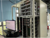
HTOL/LTOL chip-level dynamic aging electrical test equipment development and ATE CP/FT electrical test equipment integration test solution——Suzhou Xinda Semiconductor Technology Co., Ltd.


With the increasing support of China's semiconductor industry policy and the great favorable conditions of the test equipment market, a number of excellent companies with advanced technology and reliable products have emerged in China, represented by Suzhou Xinda Semiconductor Technology Co., Ltd.

Suzhou Xinda Semiconductor Technology Co., Ltd. was established in Suzhou by a team full of enthusiasm and working in the chip verification industry for more than 20 years. The founder has a master's and doctoral degree in engineering from a well-known top university at home and abroad. The Suzhou Xinda Semiconductor Technology Co., Ltd. founded by him is a solution company integrating high-end chip equipment, equipment research and development, and semiconductor design and testing.

Suzhou Xinda Semiconductor Technology Co., Ltd. is currently focusing on the development as well as subsequent corresponding software and hardware supporting testing technology services.

1686113475610.png

Please, Log in or Register to view URLs content!
 
Status
Not open for further replies.
Top