Chinese semiconductor industry

Status
Not open for further replies.

HighGround

Senior Member
Registered Member
The IC sector in play in China is that the fabless and OSAT firms are at the technological frontier, the foundries are more-or-less there as well ignoring the equipment wrinkle, most of the equipment firms lack scale but have technology and thus the main questions right now are of systems integration, working out random operational issues and the eventual deployment of the lithography scanner
That's the impression I have as well.

Scale, integration, and workflows are things that can be built up relatively quickly. Technology bottlenecks on the other hand, can be permanently crippling. The road ahead for China is arguably a lot easier, and it's still quite shocking how far China has come in solving a lot of these bottlenecks in just 3-4 years since 2019.

United States should've been far more aggressive with sanctions if we wanted to cripple China in the medium-term. The incremental approach to these sanctions have only served to "train" China in the same way that progressive overload trains weightlifters. It has also allowed China to predict where the next sanctions might hit, and build up inventory in those areas.

At this rate, it feels too little, too late on any possible response we might have. We could declare total economic war in this sector and strong-arm everyone into a total embargo. That would probably cause an economic downturn, but IMO, it also wouldn't significantly hamper China at this point. The window of opportunity was 3-4 years ago for this sort of thing to be effective. That window is gone now.
 

tphuang

Lieutenant General
Staff member
Super Moderator
VIP Professional
Registered Member
Seems to largely verify the rumors of rush ArFi shipments from ASML to China before the sanctions
Keep in mind the rush is not for all Arfi scanners, but just for those that will be blocked (2000i and above). And since you only need them for the most critical layer, there is no issue with continued import of 1980di or 1970i (my designations are not perfect here, but you get the point).

The global semi downturn has basically allowed SMIC to get earlier delivery slots. It can store them until other equipments are ready.


Anyhow, Moore threads now has its S2000 GPU validated with Jingping computing
Please, Log in or Register to view URLs content!
The importance of Moore Threads is not the product itself but just how many people are using it now. Wide spread adaptation will generally lead to success longer term. If we look at a possible future of a full Nvidia ban in China, all the current Nvidia GPU users need to have a domestic alternative that they can turn to
 

tokenanalyst

Brigadier
Registered Member

China Automotive Power Semiconductor Branch was established to build an industry standard system and ecology​


Recently, the China Automotive Chip Industry Innovation Strategic Alliance Power Semiconductor Branch (referred to as the "Branch") was established in Changsha. Dong Yang, the first chairman of the branch, said that power semiconductors are the core devices for the development of new energy vehicles, and the branch will strive to build a power semiconductor industry standard system and ecosystem.

A number of practitioners in the power semiconductor industry chain said that with the rapid development of the new energy automobile industry, there is a lot of room for the development of domestic silicon carbide power semiconductors. However, the industry is currently facing problems such as high cost in some links, insufficient effective production capacity, and insufficient standard system, and it is necessary to strengthen overall planning and industrial coordination.

The third-generation semiconductors represented by silicon carbide and gallium nitride have greater advantages in switching. The higher breakdown field strength enables them to adapt to high-voltage, high-power environments, and has good thermal conductivity. The field of new energy and new energy is gradually exerting its advantages, and the fields of new energy vehicles and photovoltaics are accelerating the application of third-generation semiconductors. However, compared with traditional silicon-based devices, the price of such devices is relatively high. The immature process production line calls for cost reduction, better production iterations, efficiency and quality of crystal growth, crystal cutting and grinding etc. to make improvements. Due to the material characteristics of the third-generation semiconductors, traditional equipment is often unable to fully adapt, and experience needs to be accumulated in the adjustment of production lines.

Cost is an important factor affecting the penetration rate of SiC semiconductors. Guo Yuhui, chip planning director of Chery Automobile R&D Institute, told the reporter of China Securities Journal that the current consensus in the industry is that IGBT (insulated gate bipolar transistor) for electric vehicles with a value of less than 200,000 yuan and silicon carbide for electric vehicles with a value of more than 200,000 yuan power semiconductors. Silicon carbide semiconductors have low loss, high pressure resistance, and high temperature resistance, which is an important development direction of power semiconductors. The industry is working together to reduce the cost of silicon carbide power semiconductors.

Zhang Zhenrong, deputy sales general manager of Sanan Semiconductor, told reporters that silicon carbide substrates account for about 60% of the cost of silicon carbide chips. Reducing the cost of silicon carbide substrates and stably increasing production are the next steps for Sanan Semiconductor. Zhang Zhenrong is full of confidence in reducing the cost of silicon carbide substrates. "It is expected that the cost of silicon carbide chips will drop by 5-8 percentage points every year." Zhang Zhenrong revealed that San'an Semiconductor will deploy an 8-inch silicon carbide wafer production line in the second phase of the project. This is one of the paths to increase production capacity and reduce costs.
 

tphuang

Lieutenant General
Staff member
Super Moderator
VIP Professional
Registered Member
Please, Log in or Register to view URLs content!
八亿时空 has created their own PHS resin for KRF photoresist and produced 50t of it last year. Looks like another part of supply chain has been solved now. In terms of materials, looks like they are quickly solving all the missing links.
 

tokenanalyst

Brigadier
Registered Member

China (Chinese equipment an material companies) pumps $7bn into upgrading chip supply chain​

Government and industry work together amid U.S. tech export restrictions

GUANGZHOU -- Chinese chipmaking suppliers plan to spend 50 billion yuan ($7.26 billion) with backing from the state to strengthen the domestic supply chain as the U.S. curbs tech exports.
"We cannot avoid decoupling in semiconductors," Chiu Tzu-Yin, president of state-backed wafer giant National Silicon Industry Group (NSIG), said at a
Please, Log in or Register to view URLs content!
hosted in Guangzhou for two days through Wednesday. "This will be the greatest opportunity for Chinese enterprises that make production machinery and materials."
As imports of foreign-made chipmaking machines have slowed due to U.S. restrictions, Chinese companies that produce chipmaking equipment and materials have gained visibility, aided by subsidies and investment under the auspices of the government's Made in China 2025 initiative.
About 35% of Chinese semiconductor factories used domestic equipment in 2022, up from 21% in 2021, Chinese media report. Domestic players have won nearly half of all public bids for equipment by leading chipmakers here so far in 2023 (more than half), a Chinese brokerage reports.

I think the author is referring to the localization rate, it was 21% in 2020 and has reached 35% this year, it could be even more higher, closer to 50%. Varies from fab to fab, some are more localized than others but in average is higher than 35%.

"Global political frictions will likely usher in a golden age to China's semiconductor manufacturing machinery sector," said David Wang, CEO of ACM Research, which specializes in wafer-cleaning equipment.
Naura Technology Group, China's top manufacturer of chipmaking devices, earned 14.6 billion yuan in revenue last year, more than six times the figure in 2017. The state-linked company bought a U.S. wafer cleaning device maker in 2018 and extended its business profile to include products for etching.
Naura Technology Group is China's biggest manufacturer of chipmaking devices. (Photo by Shunsuke Tabeta)
Naura is said to supply leading Chinese foundry Semiconductor Manufacturing International Corp. (SMIC) as well as Yangtze Memory Technologies. Naura is investing 3.8 billion yuan on building a plant in Beijing due to begin operations next year.
Advanced Micro-Fabrication Equipment, China's No. 2 manufacturer of chipmaking tools and a producer of etching devices, roughly quintupled its sales last year from 2017. Products from the state-backed enterprise can handle advanced 5-nanometer semiconductors. Construction is underway for a 1.5 billion yuan plant in Shanghai.
Sales of chipmaking equipment in China totaled 52 billion yuan last year, an industry group estimates, roughly six times more than in 2017.
About 62 billion yuan worth of chipmaking materials was sold in 2022 as well, nearly triple the 2017 figure. NSIG's revenue roughly quintupled during that span, and the company raised 10 billion yuan in funds last year alone.
"We plan to increase the monthly production capacity of 300-millimeter wafers up to 1.2 million units, quadruple the current level," Chiu said.
National Silicon Industry Group broke ground on a research hub in November 2022. (Photo courtesy of National Silicon Industry Group)
Beijing plans further support to domestic companies in light of its growing rivalry with Washington. Speculation centers on a package worth 1 trillion yuan or more.
"Upstream and downstream industries will work together on innovation, accelerating efforts for a Chinese-style self-reliance in semiconductors," said Tsinghua University professor Wei Shaojun, a policy adviser on semiconductors.
China ranked first worldwide in chipmaking equipment sales for the third consecutive year in 2022 despite a 5% decrease, industry group SEMI reports. Demand is expected to grow in 2023, especially as Chinese chipmakers anticipate new American export restrictions. SMIC plans a similar level of investment in 2023 as in 2022.
Overseas players also have an eye on opportunities in China, the world's largest market for chips. The three largest U.S. equipment makers generated around 30% of their total sales last year in China, according to Chinese research institution ChipInsights.
Sponsors for this week's Guangzhou conference included U.S.-based Applied Materials, KLA and Lam Research, as well as Germany's Siemens. A Singaporean executive from KLA used the event to highlight the company's expertise in automotive chips.
Current U.S. restrictions on tech exports to China focus on cutting-edge areas, like 10- and 14-nm logic chips. Shipments in more mature fields, like equipment, are still allowed.
One executive from a foreign company noted that losing the Chinese market would harm overall earnings, in turn impacting research and development.
From Japan, Disco and Hitachi Group were listed as sponsors for the Guangzhou event. But they kept a low profile, largely watching for U.S. moves.

Please, Log in or Register to view URLs content!
 

tphuang

Lieutenant General
Staff member
Super Moderator
VIP Professional
Registered Member
CIOMP lithography technologies developed this year.

-Ultra-high-precision lithography machine projection objective lens system wave aberration detection technology.

-Extreme Ultraviolet Lithography Optical Technology

-High-precision magnetorheological polishing technology for complex curved optical components.

-Key technologies for surface pollution prevention and non-destructive cleaning of multi-layer film optical components in EUV lithography machine.
Please, Log in or Register to view URLs content!
2023年4月13日下午,中国科学院院士、中国科学院前党组书记、院长白春礼到长春光机所调研。


在金宏书记的陪同下,白春礼先后参观了高通量基因测序仪、EUV光源、02专项等科技创新成果及研究进展,并就相关技术问题与科技人员进行了深入交流。白春礼对长春光机所光电关键核心技术攻关所取得的成绩给予了高度肯定,希望长春光机所继续发挥优良传统,为加快解决光电领域“卡脖子”问题努力作出新的更大贡献。

中国科学院院士张洪杰,长春市科协党组书记、主席周衍广及副主席王立伍陪同调研。
not sure if this is what you looked at, but CAS came to visit CIOMP a week ago and EUV light source was one key thing that was looked at. Project 02 includes EUV itself, so looks like they did accomplish something recently. I get the feeling that the prototype might get assembled over the next year.
 

tokenanalyst

Brigadier
Registered Member

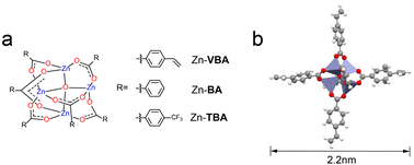
A novel stable zinc–oxo cluster for advanced lithography patterning​

Youming Si, Yingdong Zhao, Guangyue Shi, Danhong Zhou, Feng Luo, Pengzhong Chen, Jiangli Fan and Xiaojun Peng\


State Key Laboratory of Fine Chemicals, Frontiers Science Center for Smart Materials Oriented Chemical Engineering, School of Chemical Engineering, Dalian University of Technology, Dalian 116024, China
Ningbo Institute of Dalian University of Technology, Ningbo 315016, China
Research Institute of Dalian University of Technology in Shenzhen, Shenzhen 518057, China
School of Materials Science and Engineering, Nankai University, Tianjin 300350, China

Abstract​

Recently, the development of novel metal-containing resists has received much attention in extreme ultraviolet lithography (EUVL) owing to their smaller sizes and higher EUV absorptivity than traditional polymer resists. Herein, we report zinc (Zn)–VBA, a novel stable zinc–oxo cluster-based photoresist molecule with the [Zn4O]6+ inner core and six organic ligands based on 4-vinylbenzoic acid. Zn–VBA was simply prepared by the reactions between the zinc-oxide and 4-vinylbenzoic acid, exhibiting atomically precise structure and good batch stability. Based on single-crystal X-ray diffraction analysis, the size of Zn–VBA is 2.2 nm, which is in line with the high-resolution requirements for advanced lithography technology. Zn–VBA exhibits excellent thermal stability up to 400 °C, much better than the reported zinc-based clusters. Moreover, theoretical studies have revealed the roles of organic ligands in their high thermal stability. Spin-coating methods were employed to fabricate homogenous thin films of Zn–VBA, which showed a quite small roughness value in the absence of viscosifiers, as confirmed by atomic force microscopy images. More importantly, the Zn–VBA films performed well in the electron beam lithography (EBL) and EUVL tests without the addition of photoinitiators, giving prominent pattern lines. This work proves the structural advantages of benzoic-acid-based zinc–oxo clusters as promising EUV patterning materials, which inspire future exploration of metal–oxo clusters (MOCs) resist materials for advanced lithography.​
Graphical abstract: A novel stable zinc–oxo cluster for advanced lithography patterning


Please, Log in or Register to view URLs content!
 

tonyget

Senior Member
Registered Member
A russian technician working on galvanic isolation. After the sanction he cannot get American chips anymore,so he has to redesign the circuit. He discovered the TPT774x chip from 3PEAK(one of the leader of analog chips in China) can replace the US chip perfectly


And In this video,he also talked alot about he went to Russia electronic show,there is lots of Chinese companies there,and his thoughts on Chinese electronic companies entering Russian market

蜂蜜浏览器_2023-04-22_211537.jpg
 
Last edited:

tokenanalyst

Brigadier
Registered Member

The annual output of 11,000 tons of semiconductor photoresist project is about to be completed!​


Recently, Red Avenue New Materials Group Co., Ltd. released its 2022 annual report: During the reporting period, the company realized an operating income of approximately RMB 2.5 billion, an increase of 7.74% over the same period of the previous year, and realized a net profit of approximately 300 million yuan attributable to the parent, an increase of approximately RMB 300 million compared with the previous year. A decrease of 8.71% over the same period.

Red Avenue New Material’s annual output of 11,000 tons of semiconductors, flat panel display photoresist and 20,000 tons of related supporting reagents has entered the final acceptance stage of the project. It is expected that all construction will be completed in the second quarter of 2023, and then enter the trial production stage, and carry out different Customer verification of variety products.

Red Avenue New Materials focuses on the development of electronic materials business, and has become a leading enterprise in the field of photoresist production in China through the investment and acquisition of leading manufacturers in the photoresist industry and the investment and integration of the upstream and downstream of the industrial chain. During the reporting period, the company's electronic materials business mainly covered semiconductor photoresists and supporting reagents, display panel photoresists, PI materials and electronic resins and other products.

In 2022, the company's semiconductor photoresist business will achieve operating income of 176.52 million yuan (company-wide caliber), a year-on-year increase of 53.48%; the company's G/I line photoresist products for semiconductors will increase by 45.45% over the same period last year; An increase of 321.85% over the same period last year.

The main body of the semiconductor photoresist production of Red Avenue New Materials is Beijing Kehua Microelectronics, a subsidiary company. At present, the core photoresist products are I line and KrF photoresist, of which I line products can provide 0.3 μm and above, and KrF can provide 0.11 μm and above .

Please, Log in or Register to view URLs content!
 

tokenanalyst

Brigadier
Registered Member

Guangdong-Hong Kong-Macao Greater Bay Area Particle Application Technology Innovation Center Photon Counting Imaging Chip Project settled in Wuxi High-tech Zone​


The Guangdong-Hong Kong-Macao Greater Bay Area National Technology Innovation Center was unveiled in Guangzhou on April 22, 2021. It is one of the three comprehensive national technology innovation centers that are cross-regional, cross-field, interdisciplinary, and cross-industry built according to the national strategic plan. , is the country's strategic scientific and technological force in the Guangdong-Hong Kong-Macao Greater Bay Area and the "four beams and eight pillars" of the national regional innovation system.

As one of the innovation platforms directly under the National Innovation Center of the Greater Bay Area, the Particle Application Technology Innovation Center originates from the advantageous subject foundation and innovative technology accumulation of the Department of Engineering Physics of Tsinghua University . Focus on technological innovation research and development and industrialization of results that can quickly form industrial scale and economic benefits, and also focus on the construction of a platform that supports the research and development of key common technologies for particle applications. The Particle Center adheres to the coordinated development of government, industry, academia, research and application. According to the integrated plan of "Technology Innovation Center + Industrial Platform + Demonstration Application Base/Demonstration Hospital", it is coordinated and promoted, and is committed to realizing self-reliance and self-improvement of my country's particle application technology and independent industrialization of equipment. The goal is Build the most comprehensive and highest-level particle application technology innovation, achievement transfer and industrialization platform in my country.
 
Status
Not open for further replies.
Top