Chinese semiconductor industry

Status
Not open for further replies.

european_guy

Junior Member
Registered Member
China already mastered 28nm. how can they ban it?

Ok, let's say banning on 28nm is a 6-12 months in the future, maybe sooner for US companies and after some months for Japanese and ASML too.

For sake of discussion let's say second half of 2023 in the worst case for China.

Impact of banning on 28nm of

1. US companies.

Here maybe AMAT ion implantation can be a problem, current local manufacturers have just started and 1 year to iron out and polishing 28nm node in volume production is not a lot.

KLA tools. Maybe also these ones can have an impact on 28nm, but I would ask some expert here.


2. Non US companies

ASML. Of course! SMEE should come out with 28nm in volume production in less than one year time. Is a huge challenge. Volume production is not like to (secretly) run some prototypes in some lab / side line.

Japanese materials (photoresists, chemicals, photomasks, maybe even high quality wafers in volumes) could be a problem. Regarding tools, I'd guess China is fully covered already, but until we don't have a 28nm fabs fully localized we don't know for sure.

The first fully localized 28nm fab in volume production will be THE milestone.

After that Chips War can be considered won in the next couple of years. Maybe 2023 will be the year.
 

FairAndUnbiased

Brigadier
Registered Member
That's an interesting point of view. Why do you think this commercialization will necessarily precede the assembly of a prototype? I would think assembling the prototype and commercializing the component would proceed independently? Besides, what use do these components have outside an EUV lithography tool?
EUV components are highly related to earlier components.

1. Multilayer mirrors: Si/Mo version of dielectric multilayer mirrors already used in UV/vis optics.
2. Drive laser: High power CO2 laser, similar to industrial laser welders.
3. Wafer chamber: Vacuum chamber with high throughput pump, same as other vacuum chambers.
4. Wafer stage: Dual air suspension stage, used previously in other lithography instruments.
5. Hydrogen management system (for optics cleaning): similar to other hydrogen management systems in i.e. fuel cells or hydrogen handling plants.

The new component is the tin droplet management system, which isn't used anywhere else.
 

olalavn

Senior Member
Registered Member
Its not to stop China from progressing vertically in shrinking node sizes, I think those bans are used to slow china's progress horizontally like slowing down the build up of WPH capacity. So international tech companies can't jump into the Chinese semi ecosystem because of limited capacity for the next 5~10 years.
In terms of quantity, mainland China is expected to be the first in the world, and there are 20 mature process factories/production lines planned in this region
Please, Log in or Register to view URLs content!
 

PopularScience

Junior Member
Registered Member
Ok, let's say banning on 28nm is a 6-12 months in the future, maybe sooner for US companies and after some months for Japanese and ASML too.

For sake of discussion let's say second half of 2023 in the worst case for China.

Impact of banning on 28nm of

1. US companies.

Here maybe AMAT ion implantation can be a problem, current local manufacturers have just started and 1 year to iron out and polishing 28nm node in volume production is not a lot.

KLA tools. Maybe also these ones can have an impact on 28nm, but I would ask some expert here.


2. Non US companies

ASML. Of course! SMEE should come out with 28nm in volume production in less than one year time. Is a huge challenge. Volume production is not like to (secretly) run some prototypes in some lab / side line.

Japanese materials (photoresists, chemicals, photomasks, maybe even high quality wafers in volumes) could be a problem. Regarding tools, I'd guess China is fully covered already, but until we don't have a 28nm fabs fully localized we don't know for sure.

The first fully localized 28nm fab in volume production will be THE milestone.

After that Chips War can be considered won in the next couple of years. Maybe 2023 will be the year.
1. Kingston's ion implanter already archived 7nm. We have CETC too.

万业企业:万业企业旗下凯世通超越7nm离子注入平台已通过客户验证并取得验收​


Please, Log in or Register to view URLs content!

2. SMIC Jingcheng has started production. This is localized fab.
 

tokenanalyst

Brigadier
Registered Member
Here maybe AMAT ion implantation can be a problem, current local manufacturers have just started and 1 year to iron out and polishing 28nm node in volume production is not a lot.
CETC and Wanye ion implanters are for this node and below. Wanye looks promising, I posted table with the characteristic and is very close to western ones in performance.
CETC has decade of experience with high energy medium energy high current medium current ion implanters.

CETC does implanters: high energy, medium energy and medium current

Medium beam ion implanter:
Medium beam current, dose 2E11-1E16 ions/cm2
200mm/300mm, electrostatic chuck, single chip injection
Single charge 1kev-300kev, maximum triple charge 900kev
Parallel beam, horizontal and vertical 2D angle detection and correction
Special ion implanter:
Multi-element implantation: B+, P+, H+, He+, Ar+, O+, Ni+, Zr+, Mo+, Fe+, etc.;
Batch loading, single wafer injection, substrate size 3-6"
Single charge 1KeV-300KeV;
Low temperature target (liquid nitrogen cooling), normal temperature target and high temperature target (600℃) are optional.
Large beam ion implanter:
High beam current, dose 2 E 12 - 2 E 17 ions/cm2
300mm, electrostatic chuck, monolithic injection
Single charge 200ev-50KeV
200ev, B+ beam current greater than 2mA
Broadband beam, horizontal angle detection and correction
High energy ion implanter:
300mm, electrostatic chuck, single-chip injection;
Single charge 10KeV-1500KeV;
Parallel beam, horizontal angle detection and correction;
Maximum productivity, 250 pieces/hour;
Injection uniformity and repeatability can reach 0.5%.


Kingstone/Wanye enterprise: High current more precise ion implanters.

View attachment 89778

My wild guess: is that looks like a group making equipment specifically for this kind of memory production, looks like it was created in 2020, something they want but cannot by find in the open market (for obvious reasons). Probably working with CETC who act as a semipermeable barrier between the Civil and military sector by making research made by the military available to the Civil/commercial sector.
Shuoke Zhongkexin: The domestic substitution of ion implanters speeds up the pace of
original Zhao Yuanchuang core ideas1 week ago


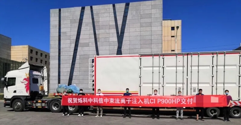
On June 15, 2020, Shuoke Zhongkexin announced that the 12-inch medium-beam ion implanter has been successfully moved into the large integrated circuit production line, which marks a new step in the marketization process of domestic ion implanters!


zkx-1.webp.jpg

The development of CMOS technology has greatly promoted the development of ion implantation (Ion Implantation) technology. It can also be said that the continuous maturity of ion implantation technology has further improved the quality of integrated circuit products, especially the performance of CMOS products. When the line width enters sub-micron , ion implantation has become an indispensable process in the entire pre-manufacturing process of integrated circuits.

In the chip production process, multiple ion implantations are required, and the implantation times are different for different chip types and process nodes. With the rapid advancement of the CMOS process, the number of ion implantations also increases rapidly. For example, in the 1970s, only 6 to 8 injections may be needed to process an n-type metal oxide semiconductor (NMOS), but now 40 injections or even more are required for 28nm logic devices.

zkx-2.webp.jpg

In the actual manufacturing process, the requirements for ion implantation are also different, such as junction depth (the energy given to ions during implantation), dose (the amount of impurities required for implantation), uniformity, repeatability, etc. All have different requirements. Generally speaking, the dose of ion implantation depends on the beam current value and time, and the implantation depth depends on the accelerating electric field. In order to meet these different needs, ion implanters with different processing capabilities are required in different links, including Medium Current ion implanters, High Current ion implanters, and High Energy ion implanters. injection machine.

There are relatively high competition barriers in the ion implanter industry for integrated circuits, and the industry concentration is relatively high. Overall, the entire market is dominated by American manufacturers. Applied Materials, Axcelis, and Advanced Ion Beam Technology (AIBT) together occupy 80% of the global market.

Driven by various policies, the research and development of ion implanters in my country has also made significant progress. A few days ago, the Beijing Science and Technology Award Work Office announced the results of the 2019 Beijing Science and Technology Award evaluation committee project evaluation results. Ion implanter suppliers Shuoke Zhongkexin and Kaishitong joined hands to participate.

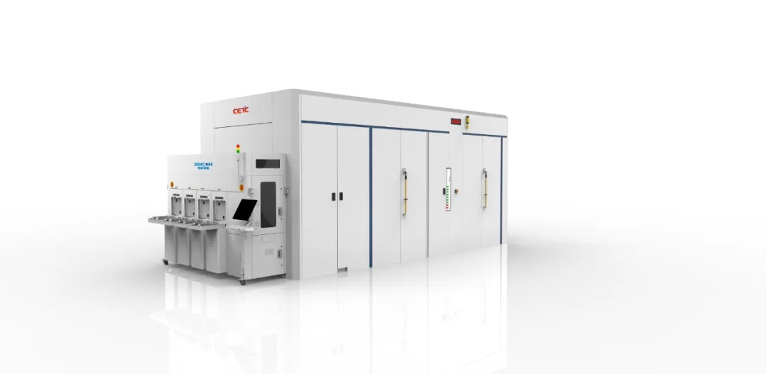
Shuoke Zhongkexin focuses on the R&D and manufacturing of ion implanters for integrated circuits, and has always been committed to solving the problem of independent controllability of key technologies of ion implanters. It has formed medium beam, large beam, high energy, special applications and third-generation semiconductors. It has a full range of ion implanter product systems, has a post-doctoral scientific research workstation, and has established an ion implanter industrialization platform that meets the requirements of SEMI standards. The annual production capacity reaches 30 units. The products are widely used in world-renowned chip manufacturers and are highly recognized by customers.


The 12-inch medium-beam ion implanter delivered this time has excellent functions in terms of angle control, dose control, and equipment process capabilities, and the overall performance of the machine has reached the international level of similar products.


The person in charge of Shuoke Zhongkexin said that catching up with the mainstream is only the beginning, and the goal is to achieve domestic substitution in a system. The series of ion implanters independently developed by the company have run a total of 6.5 million pieces on the customer's production line, stably supporting the customer's mass production. In addition, a professional after-sales service team has been established to implement a 7X24 On Call response mechanism to continuously improve customer experience and accelerate the process of localization.
Please, Log in or Register to view URLs content!

KingStoneSemi


Sir does this mean they already completed the R&D on 7nm machine? and the verification and certification will be done next year? I'm saying this cause the Chinese will only boast or promote a product IF there is a certainty that it will perform and enter production.

The founding team of KST is mainly from a world-renowned ion implanter company. It has been deeply involved in the field of ion implanters for more than 30 years. It has taken the lead in developing many best-selling ion implanters when the process technology of the integrated circuit industry is updated. With the continuous shrinking of the integrated circuit chip process process, in response to the ion implantation needs of domestic and foreign customers for advanced process chip manufacturing, KST has chosen a "one step ahead" product positioning strategy, in the "10nm and below three-dimensional device structure FinFET integrated circuit ion implanter" With the support of the scientific and technological project "R&D and Industrialization", we will develop ion implanters for cutting-edge processes (based on the beyond 7-nanometer ion implantation platform), and establish corresponding research and development platforms, core key technologies and process research parameter databases and performance testing standards.
 

tokenanalyst

Brigadier
Registered Member
KLA tools. Maybe also these ones can have an impact on 28nm, but I would ask some expert here.
Another promising area in China, companies like Angstrom-e, RSIC, Shanghai Jingce and DJAL. They have and they are launching products to cover optical metrology, Xray metrology, SEM metrology and yield management

Well, Shanghai Jihnce and RSIC offer Optical metrology equipment probably using a technique similar to KLA for thin film measurement and CD measurement, IDK for overall QC control. So is good opportunity to break through that monopoly.

Please, Log in or Register to view URLs content!

Please, Log in or Register to view URLs content!

View attachment 99620
The metrology field has been growing fast in China in the last few years.

CD-SEM
Please, Log in or Register to view URLs content!

X-Ray CD
Please, Log in or Register to view URLs content!

Optical CD.
Please, Log in or Register to view URLs content!

And that is not counting the ones in who do equipment metrology in packaging

Overall lithography is the most urgent tool in China right now and they should put a war like effort to develop a strong nano and micro patterning industry,
 

FairAndUnbiased

Brigadier
Registered Member
EUV components are highly related to earlier components.

1. Multilayer mirrors: Si/Mo version of dielectric multilayer mirrors already used in UV/vis optics.
2. Drive laser: High power CO2 laser, similar to industrial laser welders.
3. Wafer chamber: Vacuum chamber with high throughput pump, same as other vacuum chambers.
4. Wafer stage: Dual air suspension stage, used previously in other lithography instruments.
5. Hydrogen management system (for optics cleaning): similar to other hydrogen management systems in i.e. fuel cells or hydrogen handling plants.

The new component is the tin droplet management system, which isn't used anywhere else.
my mistake. wafer stage is not an air stage, duh, since its in a vacuum chamber. it is a maglev stage, which is also already in use for maglev turbo pumps on the small scale and trains at the large scale. Its 20 years old at this point.

Please, Log in or Register to view URLs content!

Please, Log in or Register to view URLs content!
 

gadgetcool5

Senior Member
Registered Member

US to Add More Than 30 Chinese Companies to Trade Blacklist​

The Biden administration plans to put Yangtze Memory Technologies and more than 30 other Chinese companies on a trade blacklist that would prevent them from buying certain American components, deepening tensions between the world’s two economic superpowers.

The US Department of Commerce will add China’s leading maker of memory chips and the others to the so-called Entity List as early as this week, according to a person familiar with deliberations who asked not to be named discussing a sensitive matter.

Companies on the Entity List are blocked from buying technology from US suppliers unless they get a special export license from Commerce. That designation’s earlier use decimated Huawei Technologies Co.’s consumer smartphone business and hampered the efforts of Semiconductor Manufacturing International Corp to grow into China’s chipmaking champion.

Please, Log in or Register to view URLs content!

It feels like late 2020 again as more of these are being announced. Only this time it's even harsher since the lowest hanging fruit is already gone.
 
Last edited by a moderator:
Status
Not open for further replies.
Top