, the rapid development of the domestic semiconductor industry has released a strong market demand for equipment. Under the influence of the complex international situation and other factors, the process of localization of equipment has been empowered.
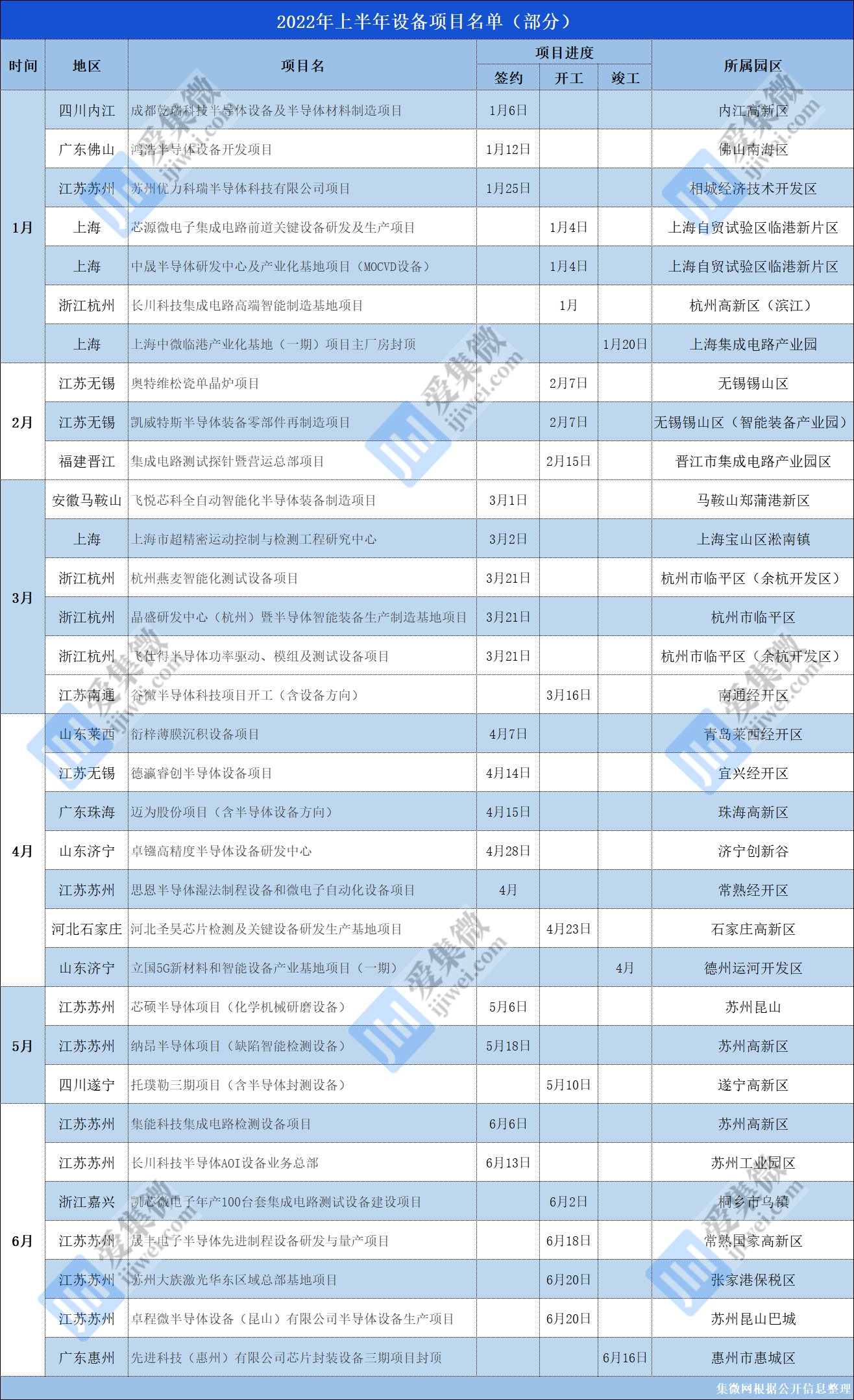
Incomplete statistics from Jiwei Network show that more than 30 equipment projects have made new progress in the first half of 2022. Among them, there were over 18 contracted projects, over 14 projects under construction, and over 2 projects entering the stage of completion and production. In terms of links, the wafer manufacturing and testing equipment projects are quite popular.

· Overview of equipment projects in the first half of 2022: Jiangsu area has dense projects, and the direction of wafer manufacturing is hot
According to statistics from Jiwei.com, the projects signed/started from January to June 2022 are mainly concentrated in the Yangtze River Delta region, accounting for over 70% of the total number of projects. Among them, most projects are in the direction of wafer manufacturing and testing equipment, accounting for nearly 70% of the total number of projects in the region.
In the Jiangsu area, equipment projects in Suzhou and Wuxi were intensively implemented and started in the first half of the year, including the first-phase investment in the Deying Ruichuang semiconductor equipment project (300 million yuan), the Changchuan Technology Semiconductor AOI equipment business headquarters project, and the advanced process of Shengfeng Electronic Semiconductor. Equipment research and development and mass production project (550 million yuan), Zhuocheng Micro Semiconductor Equipment (Kunshan) Co., Ltd. semiconductor equipment production project (300 million yuan), etc.
According to the manufacturing process, semiconductor equipment is divided into front-end wafer manufacturing equipment, packaging equipment and testing equipment, and the wafer manufacturing and testing equipment projects are more popular. According to statistics from Jiwei.com, among the equipment contracts and start-up projects from January to June, wafer manufacturing equipment accounted for 34%, followed by testing equipment accounted for 32%, and packaging equipment projects accounted for 19%.
· Overview of some projects
contract
Honghao Semiconductor Equipment Development Project
Honghao Optoelectronics invested in the construction of semiconductor precision processing plants and R&D laboratories in Nanhai District, Foshan. The project covers an area of about 50 mu, and the total planned investment is about 2 billion yuan, of which the total investment in fixed assets is 1.2 billion yuan.
Jingsheng R&D Center (Hangzhou) and Semiconductor Intelligent Equipment Manufacturing Base Project
The total investment of the project is 1.03 billion yuan, and the contract is signed in Linping District, Hangzhou, to build the Jingsheng R&D Center (Hangzhou) and the semiconductor intelligent equipment manufacturing base.
Shanghai Yanzi Thin Film Deposition Equipment Project
The project was signed with Qingdao Laixi Economic Development Zone. Shanghai Yanzi Intelligent Technology Co., Ltd. focuses on the core semiconductor process - the manufacture and production of chemical thin film deposition equipment. Its core product, VPE reactor, has been independently controllable. The Laixi project, with a total investment of 500 million yuan, will become the third semiconductor film deposition equipment company in the industry and the first in Shandong Province to connect to the production line of the chip head enterprise and realize mass production after it is put into production.
Deying Ruichuang Semiconductor Equipment Project
The project was signed with Yixing Economic and Technological Development Zone. The total investment of the first phase of Deying Ruichuang semiconductor intelligent equipment project is 300 million yuan. It will build SiC silicon carbide slicing equipment, semiconductor testing equipment, and semiconductor thin film equipment production lines.
Changchuan Technology Semiconductor AOI Equipment Business Headquarters
Changchuan Technology Semiconductor AOI equipment business headquarters project is located in Suzhou Industrial Park. It is the first independent semiconductor AOI business headquarters established by Changchuan Technology in China. It is planned that in the next five years, the number of employees in Suzhou company will reach 600, and the number of intellectual property applications will exceed 150. piece.
start
Core source microelectronics integrated circuit front-end key equipment research and development and production projects
The project is expected to have a construction period of 30 months. It will be implemented by Shanghai Xinyuan Micro Enterprise Development Co., Ltd., a wholly-owned subsidiary of the company, with a planned total investment of 640 million yuan. Photolithography process glue developing machine, immersion photolithography process glue developing machine and single-chip chemical cleaning machine and other high-end semiconductor special equipment.
Zhongsheng Semiconductor R&D Center and Industrialization Base Project
The total investment of the Zhongsheng Semiconductor R&D Center and Industrialization Base project is 540 million yuan, covering an area of 23 acres. The main investor of the project is Zhongsheng Semiconductor (Shanghai) Co., Ltd., whose business focuses on the research and development, production, sales and technical services of key MOCVD (Metal Organic Chemical Vapor Deposition) equipment and technologies for the production of second and third-generation semiconductor discrete devices.
Changchuan Technology Integrated Circuit High-end Intelligent Manufacturing Base Project
The projects that Changchuan Technology has landed in Hangzhou are mainly production capacity expansion. The project has a construction area of about 137,000 square meters. After completion, it will integrate R&D, production, office, testing, service and other functions to meet the company's high-end equipment R&D and manufacturing needs.
Shengfeng electronic semiconductor advanced process equipment research and development and mass production project
The project will be invested and constructed in two phases, and will develop semiconductor packaging and testing equipment, IC substrate manufacturing equipment, integrated circuit board printing equipment and vacuum plug hole manufacturing equipment business. Set up a research and development center and a packaging and testing center, and locate the enterprise headquarters for operation
Completion/Commissioning
The main workshop of the Shanghai Zhongwei Lingang Industrialization Base (Phase I) project is capped
The project is located in Lingang Integrated Circuit Industrial Park, Shanghai, with a total construction area of about 180,000 square meters. After 133 days, the project was successfully capped. After the project is completed, it will meet the research and development, testing and industrialization needs of integrated circuits and pan-semiconductor equipment.
Advanced Technology (Huizhou) Co., Ltd. capped the third phase of the chip packaging equipment project
The ASM project introduced in Huizhou, Guangdong was completed in mid-June, which will bring an annual production capacity of 3,000 units (sets)/year of semiconductor, LED\CMOS image sensors and other chip packaging equipment. (Proofreading / Jiang Yutong)
Incomplete statistics from Jiwei Network show that more than 30 equipment projects have made new progress in the first half of 2022. Among them, there were over 18 contracted projects, over 14 projects under construction, and over 2 projects entering the stage of completion and production. In terms of links, the wafer manufacturing and testing equipment projects are quite popular.

· Overview of equipment projects in the first half of 2022: Jiangsu area has dense projects, and the direction of wafer manufacturing is hot
According to statistics from Jiwei.com, the projects signed/started from January to June 2022 are mainly concentrated in the Yangtze River Delta region, accounting for over 70% of the total number of projects. Among them, most projects are in the direction of wafer manufacturing and testing equipment, accounting for nearly 70% of the total number of projects in the region.
In the Jiangsu area, equipment projects in Suzhou and Wuxi were intensively implemented and started in the first half of the year, including the first-phase investment in the Deying Ruichuang semiconductor equipment project (300 million yuan), the Changchuan Technology Semiconductor AOI equipment business headquarters project, and the advanced process of Shengfeng Electronic Semiconductor. Equipment research and development and mass production project (550 million yuan), Zhuocheng Micro Semiconductor Equipment (Kunshan) Co., Ltd. semiconductor equipment production project (300 million yuan), etc.
According to the manufacturing process, semiconductor equipment is divided into front-end wafer manufacturing equipment, packaging equipment and testing equipment, and the wafer manufacturing and testing equipment projects are more popular. According to statistics from Jiwei.com, among the equipment contracts and start-up projects from January to June, wafer manufacturing equipment accounted for 34%, followed by testing equipment accounted for 32%, and packaging equipment projects accounted for 19%.
· Overview of some projects
contract
Honghao Semiconductor Equipment Development Project
Honghao Optoelectronics invested in the construction of semiconductor precision processing plants and R&D laboratories in Nanhai District, Foshan. The project covers an area of about 50 mu, and the total planned investment is about 2 billion yuan, of which the total investment in fixed assets is 1.2 billion yuan.
Jingsheng R&D Center (Hangzhou) and Semiconductor Intelligent Equipment Manufacturing Base Project
The total investment of the project is 1.03 billion yuan, and the contract is signed in Linping District, Hangzhou, to build the Jingsheng R&D Center (Hangzhou) and the semiconductor intelligent equipment manufacturing base.
Shanghai Yanzi Thin Film Deposition Equipment Project
The project was signed with Qingdao Laixi Economic Development Zone. Shanghai Yanzi Intelligent Technology Co., Ltd. focuses on the core semiconductor process - the manufacture and production of chemical thin film deposition equipment. Its core product, VPE reactor, has been independently controllable. The Laixi project, with a total investment of 500 million yuan, will become the third semiconductor film deposition equipment company in the industry and the first in Shandong Province to connect to the production line of the chip head enterprise and realize mass production after it is put into production.
Deying Ruichuang Semiconductor Equipment Project
The project was signed with Yixing Economic and Technological Development Zone. The total investment of the first phase of Deying Ruichuang semiconductor intelligent equipment project is 300 million yuan. It will build SiC silicon carbide slicing equipment, semiconductor testing equipment, and semiconductor thin film equipment production lines.
Changchuan Technology Semiconductor AOI Equipment Business Headquarters
Changchuan Technology Semiconductor AOI equipment business headquarters project is located in Suzhou Industrial Park. It is the first independent semiconductor AOI business headquarters established by Changchuan Technology in China. It is planned that in the next five years, the number of employees in Suzhou company will reach 600, and the number of intellectual property applications will exceed 150. piece.
start
Core source microelectronics integrated circuit front-end key equipment research and development and production projects
The project is expected to have a construction period of 30 months. It will be implemented by Shanghai Xinyuan Micro Enterprise Development Co., Ltd., a wholly-owned subsidiary of the company, with a planned total investment of 640 million yuan. Photolithography process glue developing machine, immersion photolithography process glue developing machine and single-chip chemical cleaning machine and other high-end semiconductor special equipment.
Zhongsheng Semiconductor R&D Center and Industrialization Base Project
The total investment of the Zhongsheng Semiconductor R&D Center and Industrialization Base project is 540 million yuan, covering an area of 23 acres. The main investor of the project is Zhongsheng Semiconductor (Shanghai) Co., Ltd., whose business focuses on the research and development, production, sales and technical services of key MOCVD (Metal Organic Chemical Vapor Deposition) equipment and technologies for the production of second and third-generation semiconductor discrete devices.
Changchuan Technology Integrated Circuit High-end Intelligent Manufacturing Base Project
The projects that Changchuan Technology has landed in Hangzhou are mainly production capacity expansion. The project has a construction area of about 137,000 square meters. After completion, it will integrate R&D, production, office, testing, service and other functions to meet the company's high-end equipment R&D and manufacturing needs.
Shengfeng electronic semiconductor advanced process equipment research and development and mass production project
The project will be invested and constructed in two phases, and will develop semiconductor packaging and testing equipment, IC substrate manufacturing equipment, integrated circuit board printing equipment and vacuum plug hole manufacturing equipment business. Set up a research and development center and a packaging and testing center, and locate the enterprise headquarters for operation
Completion/Commissioning
The main workshop of the Shanghai Zhongwei Lingang Industrialization Base (Phase I) project is capped
The project is located in Lingang Integrated Circuit Industrial Park, Shanghai, with a total construction area of about 180,000 square meters. After 133 days, the project was successfully capped. After the project is completed, it will meet the research and development, testing and industrialization needs of integrated circuits and pan-semiconductor equipment.
Advanced Technology (Huizhou) Co., Ltd. capped the third phase of the chip packaging equipment project
The ASM project introduced in Huizhou, Guangdong was completed in mid-June, which will bring an annual production capacity of 3,000 units (sets)/year of semiconductor, LED\CMOS image sensors and other chip packaging equipment. (Proofreading / Jiang Yutong)


