Chinese semiconductor industry

Status
Not open for further replies.

tokenanalyst

Brigadier
Registered Member
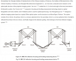
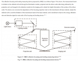
Focusing and leveling mechanism for Litho machines proposed by SMEE and IMECAS
1658851250858.png


1658851631157.png


And the prospect for EUV lithography.

4 Improvement of EUV lithography focusing and leveling measurement system​


EUV lithography machine is the core equipment for integrated circuit manufacturing at 7 nm and below technology nodes in the future. Due to the 13.5 nm exposure wavelength, it can only propagate in a vacuum. Therefore, the focusing and leveling measurement system of EUV lithography machine must be placed in a high vacuum environment [
Please, Log in or Register to view URLs content!
] . Compared with traditional dry and immersion lithography machines, in addition to the various technologies mentioned above, the focusing and leveling measurement system in a vacuum environment also needs to consider issues such as particle/gas pollution and heat dissipation control, and has a Make corresponding improvements to achieve higher measurement accuracy.

In order to control the temperature of the focusing and leveling measurement system in the vacuum chamber, Nikon Company proposed to set up a thermally conductive substrate and an active cooling device to dissipate heat by adding flowing gas between the optical element and the substrate [
Please, Log in or Register to view URLs content!
] . ASML Company proposed a method for thermal regulation of optical components operating in a vacuum environment, using gas as the medium to achieve the desired temperature by dynamically adjusting the position or direction of the cooling device [
Please, Log in or Register to view URLs content!
] . Focusing and leveling measurement systems for EUV lithography machines typically have multiple reflective optical elements, and reducing contamination on each element improves overall reflectivity. Carl Zeiss Company proposed a method for measuring the residual gas in the vacuum chamber of EUV lithography equipment, which can monitor the concentration of polluted gas, and interrupt the operation of the equipment for cleaning if necessary, and proposed a method for cleaning the pollutants in EUV lithography equipment. method, by reacting a stream of hydrogen atoms with the molecules to be cleaned to form volatile compounds that can be pumped away by a vacuum pump [
Please, Log in or Register to view URLs content!
] .

The Institute of Microelectronics, Chinese Academy of Sciences has carried out preliminary research on the adaptability of the focusing and leveling measurement system to the vacuum environment and proposed an electronic device, which places the electronic system (such as a photodetector) in a sealed shell in the vacuum chamber , effectively blocking the pollutants [
Please, Log in or Register to view URLs content!
] . Chen Jinxin et al. [
Please, Log in or Register to view URLs content!
] proposed a vacuum temperature field measurement device and method, which can not only realize the measurement in vacuum, but also improve the measurement accuracy of the temperature field. Xu Tianwei et al. [
Please, Log in or Register to view URLs content!
] proposed to place the light source of the EUV focusing and leveling measurement system outside the vacuum chamber, and transmit the light outside the vacuum chamber into the vacuum chamber through a fiber optic transmission device to supply the sensor to work, which can effectively reduce heat dissipation and vacuum. Cavity contamination [
Please, Log in or Register to view URLs content!
] .
 

tokenanalyst

Brigadier
Registered Member
Please, Log in or Register to view URLs content!

Collapse of interest alliances? The "reformists" and "revolutionaries" of the chip bill

Interestingly, it was American companies that were the first to oppose the "guardrail rule". On the eve of the test vote on the 2022 Chip Act, Intel and the U.S. Semiconductor Industry Association are already lobbying for a weakening of the "guardrail rule," which the company believes would undermine the global competitiveness of U.S. companies. An Intel spokesperson said: “Intel and many companies in our industry have worked with our industry associations to advise policymakers to ensure that we have the best legislation and are not inadvertently undermining companies that receive CHIPS funding. global competitiveness.”

If the opposition of companies such as Intel, which is a vested interest in the bill, is out of the will to improve, then the Fabless company, which has nothing to do with it, has already turned to the "revolutionary". Also before the test vote of the "2022 Chip Act", Reuters quoted people familiar with the matter as saying that if the chip bill to be voted in the Senate is only beneficial to a few chip manufacturers such as Intel and TI, AMD, Qualcomm, Nvidia and other chip designers Companies will consider opposing the bill.
 

FairAndUnbiased

Brigadier
Registered Member
If you sell a tool cheaper than a competitor but your tool is not as productive as your competitor’s tool the buyer actually loses money in their operations using your tool over a competitor’s tool. For products that are used to make things productivity to cost ratio, not purchasing price, is what matters for effective competition. In a normal situation where ASML is allowed to sell their instruments to China, China’s domestically made instruments only have an edge in purchasing price if the difference in price also makes a difference in total operation costs. So China’s tools have to become close to the same in productivity first. And that’s not just in figures like wafers per hour, but also in reliability and servicing costs.
Yep, this is why Nikon is having trouble I think. Their instruments are not as productive as ASML even in nominal WPH. Is that because of using single stage? They cost only 1/2 that of ASML but the cost difference of even 20 WPH means that they're losing, even on legacy 90 nm nodes, 20k USD per hour.

Please, Log in or Register to view URLs content!

Nikon sells at about 1/2 the cost of ASML.
 

tokenanalyst

Brigadier
Registered Member
Yep, this is why Nikon is having trouble I think. Their instruments are not as productive as ASML even in nominal WPH. Is that because of using single stage? They cost only 1/2 that of ASML but the cost difference of even 20 WPH means that they're losing, even on legacy 90 nm nodes, 20k USD per hour.

Please, Log in or Register to view URLs content!

Nikon sells at about 1/2 the cost of ASML.
ASML has become like the Nvidia of the WFE world, fabs just prefer ASML, on spec Nikon scanners don't look that unproductive, its look like they can pattern the same wafer per hour than ASML or even more, but to archive that looks like they are using pretty hefty tricks that are coming at the expense of easy of use and seamless integration, add to that the culture of ASML of closely working with fabs and semiconductor industries in different countries, just make things more difficult for Nikon.

Another thing is that productivity is also relative and complicated, lets suppose an imaginary fab needs to produce 100 WPH to satisfy their costumers orders, an 275 WPH machine looks like an overkill and overprice for them, that machine will set idle half of the time, but what if they could buy a machine that can do 150 WPH at half of the price of the 275 WPH? That machine will just fit right to them, if the lower priced machine come with a very steep learning curve, is difficult to use and can't be integrated easily, then yes go with the expensive one. but apples to apples the 150 WPH fit better the 100 WPH fab than the 250 WPH.

The monopolization of the semiconductor industry has left no middle ground. i think the fabless model become popular no just because the difficulty of fabbing on smaller process nodes but also because the rat race towards never ever increasing productivity of big players left smaller players without tools that fit their needs at the right price. I massively oversimplifying this, but you get my point.
 

FairAndUnbiased

Brigadier
Registered Member
ASML has become like the Nvidia of the WFE world, fabs just prefer ASML, on spec Nikon scanners don't look that unproductive, its look like they can pattern the same wafer per hour than ASML or even more, but to archive that looks like they are using pretty hefty tricks that are coming at the expense of easy of use and seamless integration, add to that the culture of ASML of closely working with fabs and semiconductor industries in different countries, just make things more difficult for Nikon.

Another thing is that productivity is also relative and complicated, lets suppose an imaginary fab needs to produce 100 WPH to satisfy their costumers orders, an 275 WPH machine looks like an overkill and overprice for them, that machine will set idle half of the time, but what if they could buy a machine that can do 150 WPH at half of the price of the 275 WPH? That machine will just fit right to them, if the lower priced machine come with a very steep learning curve, is difficult to use and can't be integrated easily, then yes go with the expensive one. but apples to apples the 150 WPH fit better the 100 WPH fab than the 250 WPH.

The monopolization of the semiconductor industry has left no middle ground. i think the fabless model become popular no just because the difficulty of fabbing on smaller process nodes but also because the rat race towards never ever increasing productivity of big players left smaller players without tools that fit their needs at the right price. I massively oversimplifying this, but you get my point.
The vast amount of used and refurbished KrF and dry ArF equipment from the 90s and 2000s also doesn't help. For low cost low productivity equipment you have to compete with refurbished equipment too.

The other thing is that you have to match the lowest WPH rate for any equipment in the fab. So it doesn't make sense to have a fast photolithography system if your resist developed capability or other capabilities can't catch up. Wafers in process are liabilities so you either have to throttle your good equipment, buy all best equipment, or buy more equipment.

This makes it very expensive to keep at the leading edge because you have to upgrade or expand many things at once, not pick and choose. So it seems to naturally lead to monopolies.
 

tokenanalyst

Brigadier
Registered Member
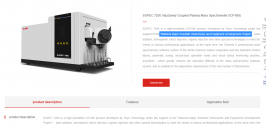
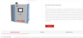
The threat of being cut off by sanctions are becoming business opportunities for some companies and people in China.

1658873441386.png

1658873570305.png


Focus Technology (Hangzhou) Co., Ltd. (stock code: 300203) was established in 2002 and is headquartered in Hangzhou, China. It is a high-tech platform enterprise with high-end equipment and product technology as its core.
Focusing Technology uses perception analysis technology and digital management to continuously protect the health and safety of the earth's environment and human life.
The company's business covers smart environment, smart industry, smart laboratory, life science and other fields, providing services for the environment, water conservancy and water affairs, emergency safety, metallurgy, petrochemical, chemical, cement, semiconductor, materials, energy, geology and mining, food and medicine, disease control, Customers in many industries such as life sciences provide innovative product portfolios and solutions such as analytical instruments, reagent consumables, information software, operation and maintenance testing services, and consulting services.
Adhering to the business philosophy of "science and technology genes, research and development cornerstones, and deep industrial cultivation", we are committed to becoming a "leading enterprise of national brands of high-end instruments and equipment".
Adhere to mastering the core technologies that are independent and controllable, constantly overcome the "neck-stuck technology", build multi-field technology platforms and innovative applications, and synchronize the development trend of the digital and intelligent era.
In the future, Focusing Technology will continue to uphold the dual-wheel drive of innovation and ingenuity, and always breathe with the times, serve all walks of life with self-controllable high-end equipment products and technologies, and jointly consolidate the foundation of scientific instrument power and embrace scientific instruments. New future!​


Please, Log in or Register to view URLs content!
 

FairAndUnbiased

Brigadier
Registered Member
The threat of being cut off by sanctions are becoming business opportunities for some companies and people in China.

View attachment 94157

View attachment 94158


Focus Technology (Hangzhou) Co., Ltd. (stock code: 300203) was established in 2002 and is headquartered in Hangzhou, China. It is a high-tech platform enterprise with high-end equipment and product technology as its core.
Focusing Technology uses perception analysis technology and digital management to continuously protect the health and safety of the earth's environment and human life.
The company's business covers smart environment, smart industry, smart laboratory, life science and other fields, providing services for the environment, water conservancy and water affairs, emergency safety, metallurgy, petrochemical, chemical, cement, semiconductor, materials, energy, geology and mining, food and medicine, disease control, Customers in many industries such as life sciences provide innovative product portfolios and solutions such as analytical instruments, reagent consumables, information software, operation and maintenance testing services, and consulting services.
Adhering to the business philosophy of "science and technology genes, research and development cornerstones, and deep industrial cultivation", we are committed to becoming a "leading enterprise of national brands of high-end instruments and equipment".
Adhere to mastering the core technologies that are independent and controllable, constantly overcome the "neck-stuck technology", build multi-field technology platforms and innovative applications, and synchronize the development trend of the digital and intelligent era.
In the future, Focusing Technology will continue to uphold the dual-wheel drive of innovation and ingenuity, and always breathe with the times, serve all walks of life with self-controllable high-end equipment products and technologies, and jointly consolidate the foundation of scientific instrument power and embrace scientific instruments. New future!​


Please, Log in or Register to view URLs content!
ICP MS is critical for trace metals testing which is a key parameter for tool acceptance and is also a major cause of yield problems.
 
Status
Not open for further replies.
Top