Oh ya..immersion. Dry dual stage is cheaper.Yes, definitely. the lockdown definitely had an impact
Is that price for the immersion dual stage or the dry dual stage?
You are using an out of date browser. It may not display this or other websites correctly.
You should upgrade or use an alternative browser.
You should upgrade or use an alternative browser.
Chinese semiconductor industry
- Thread starter Hendrik_2000
- Start date
- Status
- Not open for further replies.
It mentioned in the website
In many chinese news there is wide circulation about 28nm DUV lithography equipment by SMEE. Based on my inside industry source, all those are false.
Did that mean it doesn't even exist? Man this news is pretty sobering unless I made the wrong conclusions
That makes no sense, Re purposing an older single wafer stage stepper into dual wafer stage scanner WILL NEVER WORK, the dynamics are totally different, everything has to be designed from the ground up to accommodate new balance of masses, vibrations and so on. OF COURSE IS MORE DIFFICULT TO CONTROL. THAT POST SOUNDS JUST PLAIN STUPID.
"In the second-quarter 2022 alone, these foundries and other local peers including Yan Dong Microelectronics Technology and Triton Semiconductor together registered to purchase a total of 1,930 units of semiconductor processing machines and equipment through open tenders"
Are you referring to this section:That makes no sense, Re purposing an older single wafer stage stepper into dual wafer stage scanner WILL NEVER WORK, the dynamics are totally different, everything has to be designed from the ground up to accommodate new balance of masses, vibrations and so on. OF COURSE IS MORE DIFFICULT TO CONTROL. THAT POST SOUNDS JUST PLAIN STUPID.
上海微电子 重新设计并将所有过去的 客户无法接受 单工作平台 光刻设备转换为双工作平台
"Shanghai Microelectronics redesigned and converted all former customers who could not accept single-working platforms and lithography equipment into dual-working platforms."?
Shanghai Microelectronics redesigned and unacceptable all past customers Converting single stage lithography equipment to dual stage dual stage is more difficult to control.Are you referring to this section:
上海微电子 重新设计并将所有过去的 客户无法接受 单工作平台 光刻设备转换为双工作平台
"Shanghai Microelectronics redesigned and converted all former customers who could not accept single-working platforms and lithography equipment into dual-working platforms."?
So DWSi is $10M. Any idea how much DWS dry stage?Oh ya..immersion. Dry dual stage is cheaper.
45 wet processing equipments of China Electric Power Co., Ltd. have entered the mainstream 8-inch chip production line in China
Recently, the double 8-inch full-line automatic wet process equipment developed by the 45th China Electric Power Research Institute (hereinafter referred to as the 45th Institute) has entered the domestic mainstream FAB factory. The entire line of equipment meets the 8-inch 90nm-130nm process node, and is suitable for wet chemical processes in the 8-12-inch BCD chip process.

Wafer size and process line width represent the technological level of wet process equipment. The entire line of equipment developed by 45 meets the operation standard of 8-inch mainstream FAB factory wet process equipment, with a high degree of automation and high system integration, covering 8-inch BCD chips. The wet chemical process in the process realizes fully automatic wet degumming, wet etching, wet metal etching, RCA cleaning, Marangoni drying and other processes.
Equipment is the cornerstone of the semiconductor industry. According to SEMI statistics, global semiconductor manufacturing equipment sales in 2021 will reach a record high of US$102.6 billion, a year-on-year increase of 44%. Driven by the global expansion of chip production, fab equipment spending will continue to increase, and the global market is expected to reach $117.5 billion in 2022 and $120.8 billion in 2023.
The strong market demand has brought development opportunities for local semiconductor equipment companies. Jing Cui, chairman and secretary of the party committee of China Electronics Technology Electronic Equipment Group Co., Ltd., said that based on the characteristics of the semiconductor equipment industry "technology-intensive, talent-intensive, capital-intensive, and long return period", domestic advanced equipment enterprises have formed a "R&D first, industrial Follow-up, financial support" development model, and has the following three characteristics:
First, the semiconductor equipment industry is highly concentrated. According to the statistics of China Electronic Special Equipment Industry Association, the sales revenue of the top ten domestic semiconductor equipment companies accounts for 80% of the total sales revenue of domestic equipment companies. Equipment leading enterprises and manufacturing leading enterprises have in-depth cooperation in process and equipment development, and constantly strengthen the status of leading enterprises.
The second is the continuous enrichment of domestic semiconductor equipment subdivision varieties, gradually entering the stage of industrialization substitution. For example, Beijing Shuoke Zhongkexin Co., Ltd. has achieved independent innovation and development of a full range of ion implanters for special applications such as medium-beam, large-beam, high-energy and third-generation semiconductors, and the process segment covers 28nm.
Third, the capital market is increasingly supporting the technological innovation and industrialization of semiconductor equipment. Since 2019, many companies have used the Science and Technology Innovation Board to quickly achieve IPO listing, raise funds, accelerate scientific research investment, and further accelerate industrialization.
is this from same section with different translation? completely different feel from the two translations. Interesting.Shanghai Microelectronics redesigned and unacceptable all past customers Converting single stage lithography equipment to dual stage dual stage is more difficult to control.
But the table in the blog with tool and lens NA looks right. I think I had mentioned before SMEE's best advertised SSA600 90nm system is quite a big step away from immersion. From their papers, it's a 0.75NA system so not even the same as the modern Nikon/ASML ArF system that has 0.93NA. So on the table, we see that modern KrF systems from Canon and ASML could hit same 90nm resolution as SMEE SSA600 ArF system. So, SSA600 not as advanced or equivalent to current ArF dry system as many people think it is.
So some info correct and some incorrect. Not so atypical for blogs or articles on the web.
Last edited:
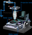
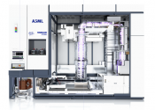
That is why i avoid posting posts from social media like twitter or rumors that people say, the part of the delivering of lithography machines to Chinese fabs is public knowledge that you can find in some financial documentation in the Chinese internet BUT the part were he says that SMEE is purposely fitting single wafers stages machines with dual wafer stages I haven't found it anywhere, i am reading from top to bottom. AND COURSE A SINGLE WAFER STAGES ARE GOING TO BE LOWER YIELD THAN DUAL STAGE,And specially comparing SMEE and ASML, unless you use a very powerful ligth source and very high speed stage.
Even the all powerful Nikon single stage I-line scanners have lower yield than the ASML dual stage one. 200 vs 230 wph. THAT IS JUST LOGIC.
Now i have a curiosity that i can't satisfy because i can't find any reliable information, just because a post of a guy in forum.
Even the all powerful Nikon single stage I-line scanners have lower yield than the ASML dual stage one. 200 vs 230 wph. THAT IS JUST LOGIC.


Now i have a curiosity that i can't satisfy because i can't find any reliable information, just because a post of a guy in forum.
- Status
- Not open for further replies.
