Sure, but it’s always going to be higher the more patterning steps you add into your process. That’s just a function of tolerance stacking statistics.Defect rate is not static and it decreases over time as the process is matured with prior skills.

You are using an out of date browser. It may not display this or other websites correctly.
You should upgrade or use an alternative browser.
You should upgrade or use an alternative browser.
Chinese semiconductor thread II
- Thread starter vincent
- Start date
Yes, impressive figures.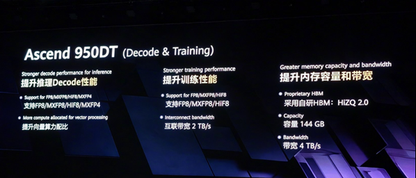
Rumor is highly credible since HW officially confirmed their proprietary HBM called HiZQ2.0. In fact the performance (144 GB 4TB) closely matches HBM3e
So Huawei might not be reliant on CXMT producing HBM3?
There isn't much coverage on the HBM situation despite being a large bottleneck. If Huawei can make their HBM itself then that's a huge win but if not, CXMT'S delay will be very problematic.
The good news is all the new money CXMT has for expansion.
The higher defect rate can be overcome by the capital cost advantage if delta is not high.Sure, but it’s always going to be higher the more patterning steps you add into your process. That’s just a function of tolerance stacking statistics.
Do you have to specially apply for a chinese brokerage account or anything?I plan to buy. Even pig can fly catching the right wind.
Higher defect rate reduces capital cost advantage. More defects means you’re throwing away wafer area. Defects are what directly determine yield. What you gain in cost advantage of scanning speed and cheaper process you are also giving up in cost disadvantage of more scanning passes and tolerance stacking errors. That’s why how much EUV and DUV to use for any fab line requires a rigorous operational optimization assessment.The higher defect rate can be overcome by the capital cost advantage if delta is not high.
Last edited:
I think you can access some chinese stock exchanges with Interactive brokers or find an China tech based etf.Do you have to specially apply for a chinese brokerage account or anything?
九峰山 lab developing new ALD Mo tech for 8-inch platform.
This is for compound semi material
This is for compound semi material
When looking into China's semi industry. We need to also take Chinese sources into consideration. HBM is something worked on by multiple players. Huawei has its own HBM packaging IPs and such, but it's not the only one. I think other players like JCET and Tongfu are also working on their own designs. Theoretically speaking, you don't even need CXMT DRAMs, you can buy them from SK or Samsung. Although in practice, I'm not sure they have enough supplyYes, impressive figures.
So Huawei might not be reliant on CXMT producing HBM3?
There isn't much coverage on the HBM situation despite being a large bottleneck. If Huawei can make their HBM itself then that's a huge win but if not, CXMT'S delay will be very problematic.
The good news is all the new money CXMT has for expansion.
Do you have to specially apply for a chinese brokerage account or anything?
I opened a foreign trade account in local Malaysia bank and can trade some China stock accounts.
Defects can be reduced by better metrology and process optimizations. The industry did that for the 7nm and 14nm nodes with multiple patterning with immersion. My guess is, what cannot be overcomed by the fab is the low throughput of a tool, is it to manufacturer to optimize the tools the meet the fab requirements.The higher defect rate can be overcome by the capital cost advantage if delta is not high.
Huada Jiutian Storage's EDA tools have been validated by leading customers and are now being used extensively in design and manufacturing.
On May 19th, Huada Jiutian stated on its investor interaction platform that its end-to-end EDA tool system for memory circuit design, after being designed and verified by leading memory chip companies, has been widely applied in the design and manufacturing of memory chips. The company emphasized that this system not only strongly supports the long-term healthy development of domestic memory chip companies but will also become an important business segment for the company.
Huada Jiutian is a leading domestic EDA software company, with product lines covering multiple fields including analog circuit design, digital circuit design, memory circuit design, flat panel display circuit design, wafer manufacturing, advanced packaging, and 3DIC design. In the crucial memory EDA sector, the company launched China's only end-to-end EDA solution for memory chips in August 2025, capable of supporting ultra-large-scale Flash/DRAM mass production. This solution provides a one-stop service from design and verification to mass production, breaking the long-standing monopoly of foreign manufacturers in this field.
Financial data shows that BGI Genomics has maintained a high level of R&D investment to solidify its technological barriers. In 2025, the company's R&D expenses reached 859 million yuan, accounting for 64.84% of its operating revenue. During the same period, the company's technical service business performed exceptionally well, achieving revenue of 201 million yuan, a significant year-on-year increase of 74.93%, becoming an important driver of revenue growth.
The successful validation and large-scale application of its storage EDA tool system by leading customers marks a significant breakthrough for Huada Jiutian in overcoming the "bottleneck" in semiconductor design software. Driven by the industry trends of self-reliance and AI, the company is accelerating its full-process product coverage through a dual-engine approach of "AI+EDA" and "3DIC," further solidifying its position as a core domestic EDA supplier.