How is it possible that they built it so fast? Crazy spredonstruction started in 2025/9
You are using an out of date browser. It may not display this or other websites correctly.
You should upgrade or use an alternative browser.
You should upgrade or use an alternative browser.
Chinese semiconductor thread II
- Thread starter vincent
- Start date
How is it possible that they built it so fast? Crazy spred
Can they rapidly build new plants each year, so that they can catch up to the market leaders very soon?
Not likely. New fab take 15 to20 months for construction.How is it possible that they built it so fast? Crazy spred
U-Precision Delivers China’s First Domestic D2W Chip-Particle Hybrid Bonding Equipment
On February 4, Beijing-based Huazhuo Precision Technology successfully delivered its independently developed D2W (Die-to-Wafer) chip-particle hybrid bonding equipment to a customer in Wuhan a landmark achievement in China’s quest for semiconductor self-reliance.
This delivery marks a major breakthrough in advanced packaging technology, a critical enabler for continuing Moore’s Law and meeting surging AI computing demands. With the global advanced packaging market projected to exceed $79.4 billion by 2030, hybrid bonding equipment essential for HBM (High Bandwidth Memory) and Chiplet integration.
Huazhuo Precision, spun out from Tsinghua University, leverages over 20 years of ultra-precision tech and core patents to fill this gap. Its new UP-D2W-HB equipment is designed for cutting-edge applications like HBM manufacturing and heterogeneous integration, directly addressing China’s urgent need for domestic high-end semiconductor tools.

This delivery is not an isolated win it’s part of a broader equipment matrix developed by Huazhuo, including:
This delivery marks a major breakthrough in advanced packaging technology, a critical enabler for continuing Moore’s Law and meeting surging AI computing demands. With the global advanced packaging market projected to exceed $79.4 billion by 2030, hybrid bonding equipment essential for HBM (High Bandwidth Memory) and Chiplet integration.
Huazhuo Precision, spun out from Tsinghua University, leverages over 20 years of ultra-precision tech and core patents to fill this gap. Its new UP-D2W-HB equipment is designed for cutting-edge applications like HBM manufacturing and heterogeneous integration, directly addressing China’s urgent need for domestic high-end semiconductor tools.

This delivery is not an isolated win it’s part of a broader equipment matrix developed by Huazhuo, including:
- Hybrid bonding (UP-UMA® HB300)
- Fusion bonding (UP-UMA® FB300)
- Laser lift-off (UP-LLR-300)
- Laser annealing (UP-DLA-300)
Together, these tools enable end-to-end, domestically controlled solutions for advanced packaging a first for China.
The milestone underscores China’s growing capacity for independent innovation in high-end semiconductor equipment, strengthening national supply chain security and supporting strategic industries like AI, memory, and high-performance computing. It represents a pivotal step toward breaking foreign monopolies and securing China’s technological sovereignty in the global semiconductor era.
The milestone underscores China’s growing capacity for independent innovation in high-end semiconductor equipment, strengthening national supply chain security and supporting strategic industries like AI, memory, and high-performance computing. It represents a pivotal step toward breaking foreign monopolies and securing China’s technological sovereignty in the global semiconductor era.
Low-altitude economy + domestically produced chips: Enabling the Jing VS839 to unlock a trillion-dollar market with its "aerial vision".
Unlike traditional solutions where cameras, thermal imagers, and rangefinders operate independently, the Weijing intelligent pod solution leverages the powerful processing capabilities of the VS839 single chip to achieve real-time fusion processing of data from three modalities: visible light, thermal imaging, and laser ranging. It can continuously observe, automatically capture images, and stably track preset targets and emergencies during low-altitude flight, providing comprehensive data support for low-altitude flight safety and efficient mission execution.

- Holographic Perception: Real-time fusion of multi-sensor data for 24/7, all-weather monitoring (even in fog, rain, or 0.001 Lux darkness).
- AI “Thinking”: 99.7% accurate target recognition (people, vehicles, drones, birds) with anti-jamming tracking and abnormal behavior detection (e.g., illegal loitering).
- Ultra-Low Latency: End-to-end delay <16ms at 4K60fps — far below industry avg. of 30ms — enabling instant response for emergency operations.
- Edge AI Power: 4 TOPS computing via quad-core A55 + dual-DSP, enabling full on-device processing — no cloud dependency.
EDA localization has entered a critical period of building "system competitiveness".
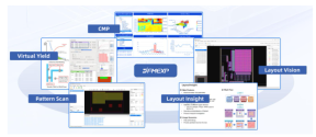
In 2025, the global EDA (Electronic Design Automation) industry entered a pivotal phase, shifting from isolated tool development to building comprehensive “system competitiveness” amid rapid technological evolution, geopolitical tensions, and surging demand for AI-driven chips. Guangli Microelectronics, a key Chinese EDA player, highlighted how the industry is no longer satisfied with single-point software breakthroughs but now demands end-to-end, integrated solutions that bridge chip design and manufacturing particularly in critical areas like Design for Manufacturability (DFM), Design for Testability (DFT), and yield optimization. This transformation reflects a broader national push for semiconductor self-reliance, turning EDA into a strategic battleground for securing a resilient domestic semiconductor supply chain.
Three major trends are reshaping the EDA landscape: first, AI is permeating every stage of chip development, from design to yield management, demanding intelligent tools that can analyze complex data and automate decisions; second, domestic players are moving beyond mere “tool replacement” to constructing closed-loop ecosystems that integrate design, testing, and manufacturing data; third, silicon photonics has emerged as a transformative new frontier, with its potential to overcome the power and bandwidth limits of traditional electrical interconnects in AI data centers. However, this emerging field suffers from immature design automation tools and low manufacturing yields, creating a strategic opening for innovators who can unify optical and electronic design capabilities. Guangli Microelectronics deployed three core strategies:
• AI-powered intelligence platforms – Launched SemiMind (a semiconductor generative AI model) and INF-AI (industrial AI analytics) to automate design verification, defect classification, and root-cause analysis, turning data silos into end-to-end intelligent decision systems.

• End-to-end lifecycle integration – Expanded from manufacturing tools to design-side capabilities by developing integrated DFM/DFT solutions tightly coupled with wafer-level testing and big data analytics, enabling a closed-loop system from design prediction to yield improvement.

• Cross-domain EDA leadership via acquisition – Acquired LUCEDA, a global leader in silicon photonics design automation (PDA), to bridge electronic and photonic chip design positioning itself as the only player offering unified “electricity + optics” EDA for next-gen AI and high-speed communication systems.
Looking ahead to 2026, Guangli Micro envisions a future defined by full-stack innovation where AI, advanced packaging (like chiplets and 3D integration), and silicon photonics converge to redefine computing infrastructure. The company is strategically aligned with these trends: its end-to-end yield optimization solutions will support China’s expanding advanced foundry capacity; its LUCEDA acquisition positions it to lead the CPO revolution; and its AI platforms empower customers to manage escalating system complexity. As the EDA industry evolves from a tool supplier to an innovation enabler, Guangli Micro aims to become a cornerstone of China’s semiconductor self-reliance, driving not just technological breakthroughs but systemic ecosystem co-development for the next generation of high-performance computing.
Jingsheng Electronics' 6-inch VB gallium oxide growth furnace has been successfully delivered to key domestic universities.
Recently, Shandong Jingsheng Electronics Technology Co., Ltd. achieved another technological breakthrough! Its independently developed and manufactured 6-inch VB crystal growth furnace (non-iridium technology) has completed full-process debugging and has been successfully delivered to key domestic universities for technology verification. This delivery represents another independent innovation achievement for Jingsheng Electronics in the field of gallium oxide crystal growth equipment, and is also an important practice for the company to deepen industry-university-research collaboration and support universities' cutting-edge materials research and development.

Glass substrates are reshaping the future of millimeter waves: Xiamen University and Yuntian Semiconductor achieve 1.2dB ultra-low loss filter.
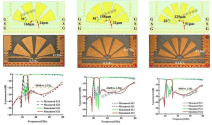
In the era of 5G/6G millimeter-wave communication, high-performance, small-size RF front-end chips have become a core bottleneck for the industry. Traditional silicon-based filters face inherent limitations in the millimeter-wave band, such as high insertion loss and difficulty in reducing size. A research team from Xiamen University, in close collaboration with Xiamen Yuntian Semiconductor Co., Ltd., has successfully developed a series of millimeter-wave bandpass filter chips based on advanced glass via technology. These chips achieve superior performance in the n257/n258 band , with insertion loss as low as 1.2dB and out-of-band rejection exceeding twice the center frequency , providing a key technological path for the miniaturization and high performance of communication equipment.

This breakthrough stems from collaborative innovation in design and manufacturing processes. Xiamen University proposed an innovative "1/n mode short-circuited ring patch" resonator structure. Through a fan-shaped design, the resonator surface area is minimized, and hybrid electromagnetic coupling is cleverly introduced to create a steep suppression zero at the passband edge. The realization of this ingenious design is thanks to the industry-leading glass via integration technology provided by Yuntian Semiconductor. The extremely low dielectric loss of the glass substrate fundamentally ensures low transmission loss, and its cost-effectiveness and 3D integration potential are significantly superior to traditional semiconductor materials. Yuntian Semiconductor's mature laser-induced etching and precision copper-filling processes ensure the quality and reliability of the high aspect ratio vias, accurately transforming design blueprints into high-performance chips. After more than six years of intensive research and development, Xiamen Yuntian is a world leader in the research and development of glass-based passive devices, and is the first company internationally to achieve mass production of glass-based 3D integrated passive devices (IPD), with products successfully applied to flagship mobile phones.
Real-world test data demonstrates the comprehensive advantages of this solution: Multiple filters developed exhibit insertion losses below 1.5dB across the 24-30GHz band, with an optimal value of 0.62dB and a typical value of 1.2dB, while achieving excellent selectivity with a 20dB suppression bandwidth exceeding twice the octave. All performance characteristics are realized on a millimeter-scale chip, achieving an optimal balance between loss, size, and suppression capability that was previously difficult to achieve simultaneously. This signifies that glass substrates now possess the capability to support the mass production of cutting-edge millimeter-wave devices.


