Translation please?
You are using an out of date browser. It may not display this or other websites correctly.
You should upgrade or use an alternative browser.
You should upgrade or use an alternative browser.
Chinese semiconductor thread II
- Thread starter vincent
- Start date
Another example is the cooperation with Guowang Optics, which is engaged in high-end optical components. Together, they tackled the exposure optical system used in lithography machines and developed equipment for 28-nanometer processes, filling a domestic gap. Through these industry-university-research cooperation, Changchun Institute of Optics, Fine Mechanics and Physics has directly made many domestically produced equipment more powerful.
TuoJing Technology SEMICON China 2025 New Product Launch Conference: Three major product series lead the innovation breakthrough of semiconductor manufacturing
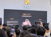
Tuojing Technology (688072) held a new product launch conference with the theme of "Tuoxinzhang·See the Future" on the first day of SEMICON China 2025, focusing on the release of new products in the ALD series, 3D-IC and advanced packaging series, and CVD series, fully demonstrating its technological breakthroughs and industrial layout in the field of semiconductor thin film deposition and advanced packaging, attracting hundreds of guests including industry leaders, media and investors to witness the event.
Hard-core technology release, defining new heights in the industry
At the beginning of the press conference, Chairman Dr. Lv Guangquan systematically elaborated on the technology development and product strategy of Tuojing Technology. He pointed out that the company has moved from front-end thin-film equipment to 3D-IC equipment based on years of technological accumulation, and the shipment of reaction chambers will exceed 1,000 units in 2024. In 2025, Tuojing will maintain high R&D investment, continue product upgrades, meet customer mass production and R&D needs, and achieve a strategic upgrade from "domestic substitution" to "technology leadership".

Subsequently, three strategic new products were unveiled one by one: Dr. Chen Xinyi, General Manager of the ALD Business Unit, stated that Tuojing has achieved the first place in ALD equipment installation volume and ALD thin film process coverage in China, and explained in detail the advantages of the new generation of atomic layer deposition equipment VS-300T in terms of floor efficiency, cost of ownership (COO), and thin film uniformity. Mr. Guo Wanli, General Manager of 3D-IC and Advanced Packaging Division, elaborated on the layout of Tojing in bonding and related products, achieving the first place in equipment installation and bonding-related process coverage in the domestic bonding field. The new product launch introduced the low-stress fusion bonding equipment Dione 300F, chip-to-wafer hybrid bonding equipment Pleione, laser stripping equipment Lyra and bonding registration accuracy measurement equipment Crux 300.
Ning Jianping, general manager of the CVD division, introduced that Tuojing Technology's CVD application capabilities have been fully recognized by the market and customers, and the current research and development direction is mainly focused on improving customer production efficiency. She pointed out that the CVD division will ship 10 new products in 2023-2024, and at the same time launch a new platform PF-300M with high production capacity and high cost performance, achieving the goal of increasing thick film production capacity, integrating processes and improving efficiency. The sharing of the three technical leaders highlights the hard-core strength of Tuojing Technology's semiconductor manufacturing technology extension and expansion.
Hard-core technology release, defining new heights in the industry
At the beginning of the press conference, Chairman Dr. Lv Guangquan systematically elaborated on the technology development and product strategy of Tuojing Technology. He pointed out that the company has moved from front-end thin-film equipment to 3D-IC equipment based on years of technological accumulation, and the shipment of reaction chambers will exceed 1,000 units in 2024. In 2025, Tuojing will maintain high R&D investment, continue product upgrades, meet customer mass production and R&D needs, and achieve a strategic upgrade from "domestic substitution" to "technology leadership".

Subsequently, three strategic new products were unveiled one by one: Dr. Chen Xinyi, General Manager of the ALD Business Unit, stated that Tuojing has achieved the first place in ALD equipment installation volume and ALD thin film process coverage in China, and explained in detail the advantages of the new generation of atomic layer deposition equipment VS-300T in terms of floor efficiency, cost of ownership (COO), and thin film uniformity. Mr. Guo Wanli, General Manager of 3D-IC and Advanced Packaging Division, elaborated on the layout of Tojing in bonding and related products, achieving the first place in equipment installation and bonding-related process coverage in the domestic bonding field. The new product launch introduced the low-stress fusion bonding equipment Dione 300F, chip-to-wafer hybrid bonding equipment Pleione, laser stripping equipment Lyra and bonding registration accuracy measurement equipment Crux 300.
Ning Jianping, general manager of the CVD division, introduced that Tuojing Technology's CVD application capabilities have been fully recognized by the market and customers, and the current research and development direction is mainly focused on improving customer production efficiency. She pointed out that the CVD division will ship 10 new products in 2023-2024, and at the same time launch a new platform PF-300M with high production capacity and high cost performance, achieving the goal of increasing thick film production capacity, integrating processes and improving efficiency. The sharing of the three technical leaders highlights the hard-core strength of Tuojing Technology's semiconductor manufacturing technology extension and expansion.
West Lake Instruments, launched the company's new silicon carbide substrate laser stripping equipment SPARC100 at the "Automotive and Photovoltaic Storage and Charging SiC Application and Supply Chain Upgrade Conference" held in Shanghai.
West Lake University, gave a speech entitled "Advanced Optoelectronic Technology to Promote Industrial Innovation". He said that the pain point facing the SiC industry today is the high cost of substrate preparation. There are two major bottlenecks in reducing the cost of silicon carbide substrates, in addition to crystal growth, there is also ingot cutting. The core product independently developed by West Lake Instruments, the SiC substrate laser stripping equipment, can reduce material loss in the production process of silicon carbide substrates, increase processing speed, and help reduce the cost of silicon carbide.
West Lake University, gave a speech entitled "Advanced Optoelectronic Technology to Promote Industrial Innovation". He said that the pain point facing the SiC industry today is the high cost of substrate preparation. There are two major bottlenecks in reducing the cost of silicon carbide substrates, in addition to crystal growth, there is also ingot cutting. The core product independently developed by West Lake Instruments, the SiC substrate laser stripping equipment, can reduce material loss in the production process of silicon carbide substrates, increase processing speed, and help reduce the cost of silicon carbide.
I am not going to comment on this one. I have nothing to say anymore except admiring the equipment.
Xingji Micro-Equipment: Advanced packaging expansion is going smoothly and production is full
1) the company's IC substrate has reserved 3-4μm resolution capabilities;
2) advanced packaging equipment has advantages in rewiring, interconnection, intelligent correction, etc., and PLP board-level packaging equipment is also deployed;
3) The etching process for lead frames has covered downstream customers such as Lide Semiconductor;
4) In the field of mask plate making, the first mask plate making equipment that meets the needs of mass production of 90nm node plate making has been verified by the client;
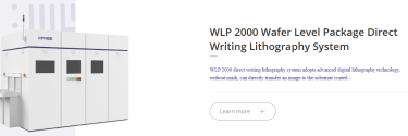
5) New display models are also actively entering the customer supply chain. Since 2024, the company has blossomed in the field of advanced packaging. In February, it delivered continuous repeat orders for WLP2000 direct writing lithography equipment to mainland advanced packaging customers; in March, it launched WA 8 wafer alignment machine and WB 8 wafer bonding machine; in August, MLF series direct writing lithography equipment was exported to Japan for the first time. According to the company's WeChat official account, Xingji Micro-Equipment WLP 2000 wafer-level direct writing lithography equipment has received repeated orders from middle-level customers and shipped. The equipment can achieve an L/S of 2μm, providing customers with solutions for the 2.xD packaging lithography process. In addition, the WLP series has been accepted and mass-produced by multiple customers in the advanced packaging market.

you mean SiCarrier surprise entry into SME equipment.. today they released entire supply line of semi tools except Lithography.. 30+ different tools from PVD, CVD, ALD, RTP, EPI, Etchers + inspection equipment, measurement products , Metrology , ion , detection products. they also give hint about Lithography.I am not going to comment on this one. I have nothing to say anymore except admiring the equipment.
just in one shot they cover entire supply chain.. WHATTTTT
never seen anything like this.. it is History
The cope is surreal among the stooges.
For us is not like is nothing new, we already knew that Chinese companies set themselves in the business of replacing US tools companies due US export controls.
Is not only SiCarrier, there is multiple vendors for same tools in a single country. Remember folks, fabs tools make the bulk of semiconductor fabrication cost. If China can have access to tools at a cheaper price than the rest of the world, is over. Fab managers from Taipei to Ohio are going to cuestion the prices of US-EU-Japan made tools, who need their high prices to keep their insane valuations.
Lithography is supposedly the last bastion of the stooges and but we already know that lithography in China is almost a done deal.


