Chinese semiconductor thread II

jli88

New Member
Registered Member
Thanks for point it out, but there is something not clear.

Here is the full screenshot you posted:

View attachment 129337

See the last note: utilization rate = total wafer / quarterly capacity

If capacity is 815K wpm X 3 months = 2445K and total wafer is 1795K it means, according to note(1)

utilization rate = 1795K / 2445K = 73%

But they calculated an utilization rate of 80.8%.

....maybe capacity is intended as capacity at the end of the quarter, they increased capacity along the quarter. But in this case the note(1) is not clear at all, because to calculate utilization rate they use the wafer shipped along the whole quarter and so they should use average capacity in the quarter, not capacity at the end of the quarter.

Thanks for pointing it out, I noticed that too. But then I thought maybe the simplistic calculation I was doing was not right. As you said, it could be end of quarter capacity. There could also be more complications, like perhaps yields and all getting in. If a wafer say is produced, but not shipped due to some reason (maybe bad)? I have no clue, not a hardware guy, but always open to learning if someone can explain.
 

dingyibvs

Junior Member
Thanks for point it out, but there is something not clear.

Here is the full screenshot you posted:

View attachment 129337

See the last note: utilization rate = total wafer / quarterly capacity

If capacity is 815K wpm X 3 months = 2445K and total wafer is 1795K it means, according to note(1)

utilization rate = 1795K / 2445K = 73%

But they calculated an utilization rate of 80.8%.

....maybe capacity is intended as capacity at the end of the quarter, they increased capacity along the quarter. But in this case the note(1) is not clear at all, because to calculate utilization rate they use the wafer shipped along the whole quarter and so they should use average capacity in the quarter, not capacity at the end of the quarter.
Does wafer shipped account for yield?
 

tokenanalyst

Brigadier
Registered Member

The total amount will reach 150 million yuan, and Beiyi Semiconductor completed the B+ round of financing​

Semiconductor Industry Network learned: On May 8, Beiyi Semiconductor Technology (Guangdong) Co., Ltd. (hereinafter referred to as "Beiyi Semiconductor") announced that it successfully completed the B+ round of financing. This round of financing will be mainly used for further research and development of SiC MOSFET technology, as well as the upgrade and expansion of production lines.

It is reported that this round of financing is led by Shanghai Wutong Private Equity Fund Management Co., Ltd., and the total amount of financing in this round is expected to reach 150 million yuan. Among them, 100 million yuan of funds has been secured, and another 50 million yuan of investment is in the final stages.

Beiyi Semiconductor stated that this round of financing will be mainly used for further research and development of sic mosfet technology, as well as the upgrade and expansion of production lines. On the one hand, by increasing R&D investment, we accelerate the pace of technological innovation and improve the performance indicators and production efficiency of sic mosfet; on the other hand, through the upgrading and expansion of production lines, we increase production scale, meet market demand, and promote the sic mosfet industry. ization process. These measures will not only help enhance the core competitiveness of Beiyi Semiconductor, but will also inject new impetus into the development of the entire semiconductor industry. This milestone achievement not only injects new vitality into the sustained and healthy development of Beiyi Semiconductor, but also demonstrates its research and development of third-generation semiconductor materials-silicon carbide (SIC) metal oxide semiconductor field effect transistor (MOSFET). and firm steps on the road to industrialization.

Please, Log in or Register to view URLs content!
 

tphuang

Lieutenant General
Staff member
Super Moderator
VIP Professional
Registered Member
Thanks for point it out, but there is something not clear.

Here is the full screenshot you posted:

View attachment 129337

See the last note: utilization rate = total wafer / quarterly capacity

If capacity is 815K wpm X 3 months = 2445K and total wafer is 1795K it means, according to note(1)

utilization rate = 1795K / 2445K = 73%

But they calculated an utilization rate of 80.8%.

....maybe capacity is intended as capacity at the end of the quarter, they increased capacity along the quarter. But in this case the note(1) is not clear at all, because to calculate utilization rate they use the wafer shipped along the whole quarter and so they should use average capacity in the quarter, not capacity at the end of the quarter.
I wouldn’t think too much about this. There are factors like production ramp up as well as Chinese new years and 29 days February which may have affected this. We don’t know exactly how they determine the monthly capacity.
 

tokenanalyst

Brigadier
Registered Member

Jingsheng Co., Ltd.: 8-inch SiC crystal growth equipment has been shipped in batches​


The silicon carbide industry is currently in the stage of transformation from 6 inches to 8 inches, and 8 inches will replace 6 inches faster than expected. Jingsheng noticed that the new orders and forward layout of leading foreign industry companies have shifted to 8 inches. Driven by the international market, Jingsheng 's domestic customers have also begun to make appropriate adjustments in new production capacity layout based on their own technological progress and yield levels.

The company's 8-inch silicon carbide crystal growth equipment has been shipped in batches. Judging from the projects currently under discussion, customers have greater intentions and demands for 8-inch equipment. However, because the company does not include the part that has not received advance payment into the statistics of orders on hand, the demand for some 8-inch equipment has not yet been counted in the orders on hand.

1715282488937.png

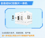
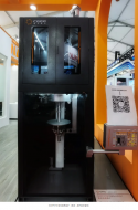
Since two years ago, Jingsheng has laid out some key products for which its cooperative clients are still dependent on imports, including the silicon carbide epitaxial furnaces and cutting machines. These two products are also core and important equipment in the entire silicon carbide industry.In terms of extension, we conducted in-depth research on the mainstream equipment in the market in the early days, and finally chose two routes: single-chip microcomputer and multi-chip microcomputer. At present, the country is dominated by single-chip microcomputers, and its process is relatively mature, so it can be quickly started and produced effectively; there is still little experience in using multi-chip microcomputers in China, but once the multi-chip epitaxial process can achieve a breakthrough, its yield rate will , cost and output efficiency are the biggest advantages. The company has now completed the preliminary development work of the epitaxial equipment prototype, and plans to send it to the client for process verification after conducting relevant tests internally.In terms of cutting equipment, Jingsheng adopts a design that is compatible with mortar and diamond wire. The company's internal trial cutting process has been tested with good results, and the equipment has now been shipped to customers. Next, for these two types of products, we will increase cooperation and efficiency in process testing with customers, strive to reach mass production level this year, and aim to enter the first echelon of the industry as our future goal.

Please, Log in or Register to view URLs content!
 

tokenanalyst

Brigadier
Registered Member

With A Total Investment Of 3.5 Billion Yuan, Construction Of A New Semiconductor Material Manufacturing Base Project In Shiyan, Hubei Province Started​


According to Shiyan Daily, Shiyan City recently held a centralized start-up event for major projects in the city in the second quarter of 2024. Among them, Hubei Guoda New Materials Group Co., Ltd.’s semiconductor new materials manufacturing base project has started.
It is reported that the project is located in Shiyan High-tech Development Zone, covering an area of 200 acres. Hubei Guoda New Materials Group Co., Ltd. invested 3.5 billion yuan. It mainly builds semiconductors such as high-purity quartz purification and processing for quartz crucibles and spherical silica powder preparation for chip packaging. New material-related product manufacturing production lines, as well as ancillary facilities such as the Semiconductor New Materials Research Institute, the Mineral Materials Testing Center, and the living area for scientific researchers.

The project is constructed in two phases. The first phase invests 1.5 billion yuan and covers an area of 100 acres to build a fully automated high-purity quartz purification production line with an annual output of 20,000 tons with completely independent intellectual property rights. The second phase investment is 2 billion yuan, covering an area of 100 acres, to build a high-purity quartz purification production line with an annual output of 50,000 tons and a high-purity spherical silica powder production line with an annual output of 50,000 tons for chips. After the project is fully completed and put into operation, it is expected to achieve an annual output value of 6 billion yuan, tax revenue of 600 million yuan, and create employment for more than 700 people.​

Please, Log in or Register to view URLs content!
 
Top