Chinese semiconductor thread II

tphuang

General
Staff member
Super Moderator
VIP Professional
Registered Member
yes. its Fab 3 that running on 100% domestic equipment and they are going to expand it further. YMTC going to add 100k to 135k WPM in next 18 months.
How do you know Fab 3 is running 100% domestic equipment and not in fab 2? How do you know it's going to add 100 to 135k wpm in next 18 months?

Harbin Founded Suzhou Extreme Ultraviolet Semiconductor Co., Ltd is making progress on Commercial EUV Light Sources.​


Suzhou Extreme Ultraviolet Semiconductor Co., Ltd. has successfully developed a 120W extreme ultraviolet (EUV) light source prototype — a critical breakthrough in China’s quest to overcome the long-standing technological bottleneck in EUV lithography equipment. As EUV lithography is essential for manufacturing advanced chips, global supply restrictions have made domestic EUV light source development a national strategic priority. Founded in 2022, the company, led by plasma expert Professor Zhang Xingqiang, has achieved key milestones including successful discharge tests and filed core patents for innovations like the “dual vacuum light source design” and “capillary discharge plasma-coupled structure,” which enhance output power and purity while reducing operational complexity.

With a 120W output meeting baseline EUV lithography requirements, the company aims to supply domestic chipmakers like SMIC and Shanghai Microelectronics, offering solutions 15–30% cheaper than global leaders ASML and Nikon, while maintaining strong margins. Targeting commercialization by 2026 and mass production by 2030, Suzhou EUV is now seeking financing to refine its prototype and accelerate industrialization. The breakthrough represents not just a technological leap but a pivotal step toward China’s semiconductor self-reliance, with plans to list on the STAR Market. This achievement signals major progress in decoupling China’s chip industry from foreign dependencies.

View attachment 168902
so for something that seems like quite relevant here, do you mind posting a link of where this translation comes from?
 

tokenanalyst

Lieutenant General
Registered Member
How do you know Fab 3 is running 100% domestic equipment and not in fab 2? How do you know it's going to add 100 to 135k wpm in next 18 months?


so for something that seems like quite relevant here, do you mind posting a link of where this translation comes from?
Is quite an advancement but they still have work to do. probably a few years more.

Please, Log in or Register to view URLs content!
 

tokenanalyst

Lieutenant General
Registered Member

Extreme Molybdenum Chip and Nanjing University are featured in Science again: Customized equipment overcomes the dynamic challenges of mass production of two-dimensional semiconductors.​


On January 30, 2026, Nanjing University and Extreme Molybdenum Core Technology (JMC) published a landmark achievement in Science, marking the second time in three months that their collaboration has been featured in the journal a rare honor signaling China’s leap from lab-scale to industrial-scale production of 2D semiconductors.

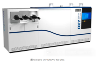
The breakthrough centers on precise control of growth kinetics for large-area, high-purity 2D materials (like MoS₂), achieved through the custom-designed Oxy-MOCVD 200 ultra equipment fully localized and developed in China. This system introduces two key innovations:
  1. Oxygen-assisted pre-reaction kinetics regulation, and
  2. Hydrogen-free, low-carbon sulfur transport, eliminating carbon contamination and enabling uniform, high-rate growth.
1769829349575.png
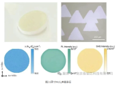
This enables the first-ever mass production of 6-inch single-crystal MoS₂ wafers, overcoming longstanding bottlenecks in crystal domain size, growth speed, and material purity.
1769829382356.png

The achievement completes a closed-loop industrialization ecosystem:
  • Substrate engineering (previously cracked in Oct 2025) + growth kinetics control = end-to-end control from substrate to material.
  • 100% domestic equipment now leads global process innovation shifting China’s role from “follower” to “definer” of semiconductor tech standards.
  • Enables next-gen applications: micrometer-scale chips, flexible displays, and post-Moore’s Law electronics.

JMC and Nanjing University are now pioneering a new model “deep synergy between process and equipment” positioning China not just as a manufacturer, but as the architect of the next generation of semiconductor technology.

Please, Log in or Register to view URLs content!
 

tokenanalyst

Lieutenant General
Registered Member

Jingsheng Electronics: Net profit for 2025 is expected to increase by 181.97%–192.21% year-on-year.​


Jingsheng Electronics is forecasted to achieve a remarkable year-on-year increase in net profit of 181.97% to 192.21% for 2025, with attributable profits expected to reach RMB 80–90 million. This surge is driven by the company’s strategic pivot toward domestic semiconductor equipment substitution, particularly in metrology technologies for advanced semiconductor processes. The firm has successfully transitioned from heavy R&D investment into tangible commercialization, with key products such as film thickness measurement, OCD, and electron beam inspection equipment now achieving large-scale mass production. These advancements have significantly boosted delivery capacity and revenue recognition, while improved operational efficiency and a stronger business mix have propelled profitability across its semiconductor segment.
1769829786334.png
1769829824226.png


The company’s leadership in China’s semiconductor metrology market is underscored by its progress in advanced nodes: core products have already been successfully deployed at the 7nm process level, with verification underway for even more advanced nodes. Notably, its bright-field optical defect inspection equipment has received client acceptance at both 14nm and 28nm nodes, signaling strong adoption in cutting-edge manufacturing. As advanced process products now constitute a growing share of revenue and orders, they have become the primary engine of Jingsheng’s financial performance. The firm is capitalizing on China’s broader push for semiconductor self-reliance, positioning itself as a critical domestic supplier in a sector undergoing rapid technological and industrial transformation.

Beyond semiconductors, Jingsheng Electronics is also benefiting from a recovery in the flat panel display industry, fueled by expanded production lines—particularly G8.6 LCD and medium-to-large OLED facilities driving demand for its testing equipment. Leveraging deep customer relationships and technological expertise, the company is expanding its footprint in traditional display markets while venturing into emerging areas such as precision optical instruments and automotive electronics. This diversification, coupled with a streamlined customer and product portfolio, has led to a substantial order backlog and a marked improvement in gross margins. With both semiconductor and display segments delivering strong growth, Jingsheng Electronics is poised for sustained expansion, reflecting confidence in its technology-driven business model and the broader industrial upgrade trajectory in China.

Please, Log in or Register to view URLs content!
 

interestedseal

Junior Member
Registered Member

Harbin Founded Suzhou Extreme Ultraviolet Semiconductor Co., Ltd is making progress on Commercial EUV Light Sources.​


Suzhou Extreme Ultraviolet Semiconductor Co., Ltd. has successfully developed a 120W extreme ultraviolet (EUV) light source prototype — a critical breakthrough in China’s quest to overcome the long-standing technological bottleneck in EUV lithography equipment. As EUV lithography is essential for manufacturing advanced chips, global supply restrictions have made domestic EUV light source development a national strategic priority. Founded in 2022, the company, led by plasma expert Professor Zhang Xingqiang, has achieved key milestones including successful discharge tests and filed core patents for innovations like the “dual vacuum light source design” and “capillary discharge plasma-coupled structure,” which enhance output power and purity while reducing operational complexity.

With a 120W output meeting baseline EUV lithography requirements, the company aims to supply domestic chipmakers like SMIC and Shanghai Microelectronics, offering solutions 15–30% cheaper than global leaders ASML and Nikon, while maintaining strong margins. Targeting commercialization by 2026 and mass production by 2030, Suzhou EUV is now seeking financing to refine its prototype and accelerate industrialization. The breakthrough represents not just a technological leap but a pivotal step toward China’s semiconductor self-reliance, with plans to list on the STAR Market. This achievement signals major progress in decoupling China’s chip industry from foreign dependencies.

View attachment 168902
So now we have confirmed EUV light source teams working on DPP, LPP, SSMB, FEL and HHG with varying degrees of progress. Within LPP, we also have at least three teams working on three drive laser types: CO2 laser (most mature tech SiCarrier), 1 micron solid state laser and 2 micron solid state laser (SIOM).
中国科学院上海光学精密机械研究所林楠研究员团队成员,胡桢麟博士在本次论坛上发表报告,分享了团队在1微米固体激光驱动锡等离子体极紫外(EUV)光源领域的研究进展。
Please, Log in or Register to view URLs content!
 

latenlazy

Brigadier
So now we have confirmed EUV light source teams working on DPP, LPP, SSMB, FEL and HHG with varying degrees of progress. Within LPP, we also have at least three teams working on three drive laser types: CO2 laser (most mature tech SiCarrier), 1 micron solid state laser and 2 micron solid state laser (SIOM).

Please, Log in or Register to view URLs content!

Both solid state laser approaches are a single team I think. 1 micron solid state laser has optical opacity issues in the excitation mechanism (excitation at that wavelength generates too much emissions outside your target wavelength), and 2 micron is one of a number of different follow up ideas to try to get around that problem.
 
Top